NordsonDAGE-SMTAI-2014.pdf
X-RAY / BON DTESTER RELIABI LITY STUD Y OF BGA DEVICES – IMP ACT OF INTERFA CIAL VOIDI NG John Tingay and Evstatin Krastev Nordson DAGE Concord, CA, USA evstatin.krastev@nordsondage.com john.tingay@nordsondage.com ABSTRA…
X-RAY / BONDTESTER RELIABILITY STUDY OF BGA DEVICES – IMPACT
OF INTERFACIAL VOIDING
John Tingay and Evstatin Krastev
Nordson DAGE
Concord, CA, USA
evstatin.krastev@nordsondage.com john.tingay@nordsondage.com
ABSTRACT
The impact of voiding on BGA/CSP joint reliability has
been discussed actively during the last several years. IPC-
610-A and J-STD-001 state that voiding greater than 25% of
the area of the solder joint as seen by top down view 2D X-
ray inspection should be considered as a defective joint.
Several studies during the last years have tried to find a
correlation between the void size and BGA solder joint
reliability (References 3-5). All these studies have utilized
2D X-ray voiding calculations that provide very precise
quantitative measurement of the total voiding within the
solder joint. However, this type of measurement does not
provide information on the exact location of the voiding
within the joint. Therefore, the impact of the void location
on the joint reliability has not been studied so far.
Naturally, if the voiding is concentrated predominantly at
the joint interfaces, we are much more concerned that a field
failure will occur in the near future.
As discussed, so far there have been no quantitative studies
that explain the impact of interfacial voiding on joint
reliability and compare this to the impact of the voiding that
is located within the bulk of the solder joint. A novel
technique called Large Board Computer Tomography, Large
Board CT or PCT, as described in Ref. 1, is capable of
providing quantitative and precise information for void
location and size, while performing the testing in a
completely non-destructive fashion. This previous study
also suggests that there is a poor correlation between total
voiding as per 2D X-ray measurements and interfacial
voiding as determined by Large Board CT. Thus, we
decided to combine the Large Board CT together with the
well-established technique of Bondtest Shear in an effort to
study the impact of interfacial voiding on the bond strength
as determined by the shear force.
For this study, we concentrated on a single BGA device that
consisted of 374 joints. We found that interfacial voiding
does degrade the strength of the BGA joints. Interfacial
voiding of 6% to 10% resulted in about 10% weaker bonds.
As a future work, we plan to expand the study using large
set of BGA devices to achieve better statistical significance.
To speed up the testing we plan to employ various levels of
automation for both the Bondtester and X-ray
measurements.
Key words: X-ray inspection, Bondtester, Shear, Voiding,
IPC-610, J-STD-001, AXI, Automated X-Ray Inspection,
X-ray technology, Computer Tomography, CT, PCT, CT
without cutting, Large Board CT.
INTRODUCTION
Calculation of voiding percentage is a standard quality
assurance procedure within the testing regime of the
microelectronics/PCB manufacturers. It is ‘regulated’ by
IPC-A-610 that states that voiding less than 25% as
determined using top view provided by regular 2D X-ray
inspection is acceptable for certain class of BGA devices –
see Figure I-1.
Figure I-1. 2D voiding calculation of a BGA device as per
IPC-A-610
This procedure gives us an indication of total voiding within
the solder joints but does not give a good representation of
the interfacial voiding that is at the BGA joint to PCB
interface. It is suggested in the literature that the interfacial
voiding could be crucial for the joint strength/quality and
does not correlate well to the total voiding as calculated by
IPC-610 (Figure I-2).
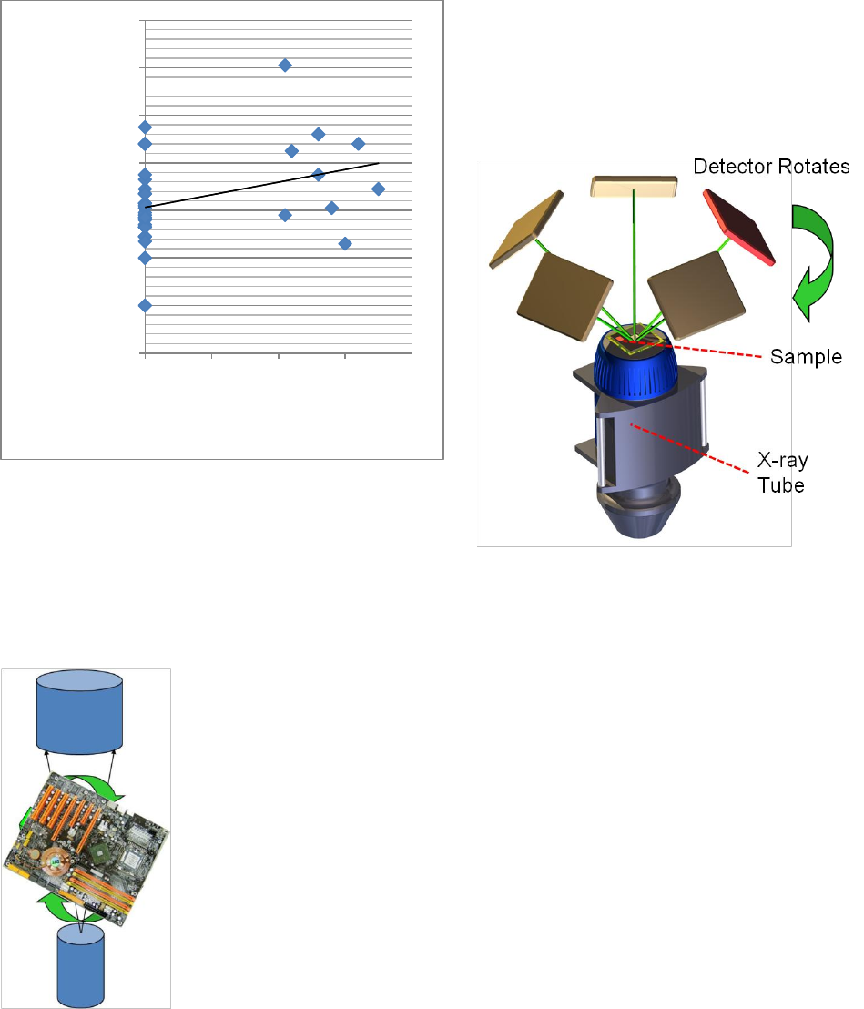
Figure I-2. Total Voiding vs. Interfacial Voiding of BGA
device as per study [1]. Very week correlation between
Interfacial voiding and Total Voiding (IPC-610) is evident-
(R
2
=0.12)
The only way to study interfacial voiding in a non-
destructive fashion is by employing Large Board CT. This
novel technique is described in detail in References [1] and
[2]. Basic principle is shown in Figure I-3 and I-4.
Figure I-3. µCT limitations for larger samples
It is obvious from Figure I-3 that the standard µCT
technique employed for the Electronics industry is not
suitable for large samples like PCB assemblies. As the
sample needs to be rotated between the X-ray source and the
detector, the large size of the PCB places the BGA device of
interest very far away from the X-ray source that results in
very low Magnification/Resolution. This is pure Physics
consideration that is valid for all X-ray CT systems.
In order to overcome this problem, the Large Board CT
technique (also called PCT) keeps the PCB flat and close to
the X-ray source while turning the detector at an angle.
This permits very good resolution images to be collected
without cutting down the valuable PCB. See Figure I-4.
Figure I-4. Basic principle of Large Board CT also called
limited angle CT or PCT.
In this study we are presenting a technique that combines
the strengths of the Large Board CT with the mechanical
testing capabilities of a standard Bondtester machine.
Current Bondtesters are extremely capable machines that
can perform a very large variety of material testing
applications like a 3 and 4 point bend test. We measure
bond strength using mechanical shear testing and try to
correlate the results to interfacial voiding as observed by
Large Board CT.
EXPERIMENTS
Using Large Board CT we examined a large a number of
PCBs looking for a BGA device suitable for our tests. This
was accomplished completely non-destructively as the
technique permits the use of a very large PCB sample. We
needed to find a device that possessed significant levels of
interfacial voiding. Finally, we were able to identify a BGA
device that had a significant number of pins that exhibited
6% to 10% interfacial voiding as well as many pins that did
not have voiding or had very low levels of interfacial
voiding - up to 1% on average. Total number of joints is
374, average ball diameter 0.65 mm and pitch 1 mm. We
y = 0.5314x + 6.1227
R² = 0.119
0.0
2.0
4.0
6.0
8.0
10.0
12.0
14.0
0.0 1.0 2.0 3.0 4.0
Total Voiding as per 2D X-ray data
(IPC-610)
Interfacial Voiding % as per Large Board CT
data
carefully scanned the device in question using Large Board
CT in order to produce a detailed map of the interfacial
voiding percentage at the PCB interface. Once done, we
started polishing down the device in order to reveal the
solder joints and prepare for the shear testing. This process
needs to be carried out very slowly and carefully in order
not to disturb the joint’s integrity. Before proceeding with
the shear testing, we grouped the pins in two groups: Group
1 - pins that exhibited 6% to 10% interfacial voiding and
Group 2 - pins with up to 1% on average interfacial voiding.
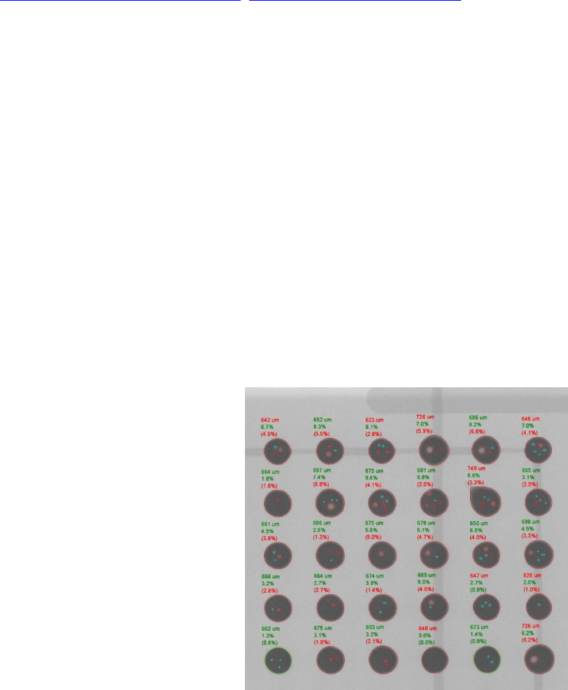
In order to do this we used electronic cross section data as
obtained by Large Board CT. Figure 1 shows a typical
electronic cross section or e-section of the interfacial area of
a BGA device. On Figure 1a the voids appear as the black
oval areas within the joint represented in white. On Figure
1b we show a typical voiding calculation carried on an e-
section at the interfacial area of the BGA device.
(a)
(b)
Figure 1. Electronic cross sections (e-sections) of interfacial
area of a BGA device. Black oval areas represent the
voiding (a), (b) BGA voiding calculation on an e-section at
the PCB interfacial area. These sections are obtained in a
completely non destructive way.
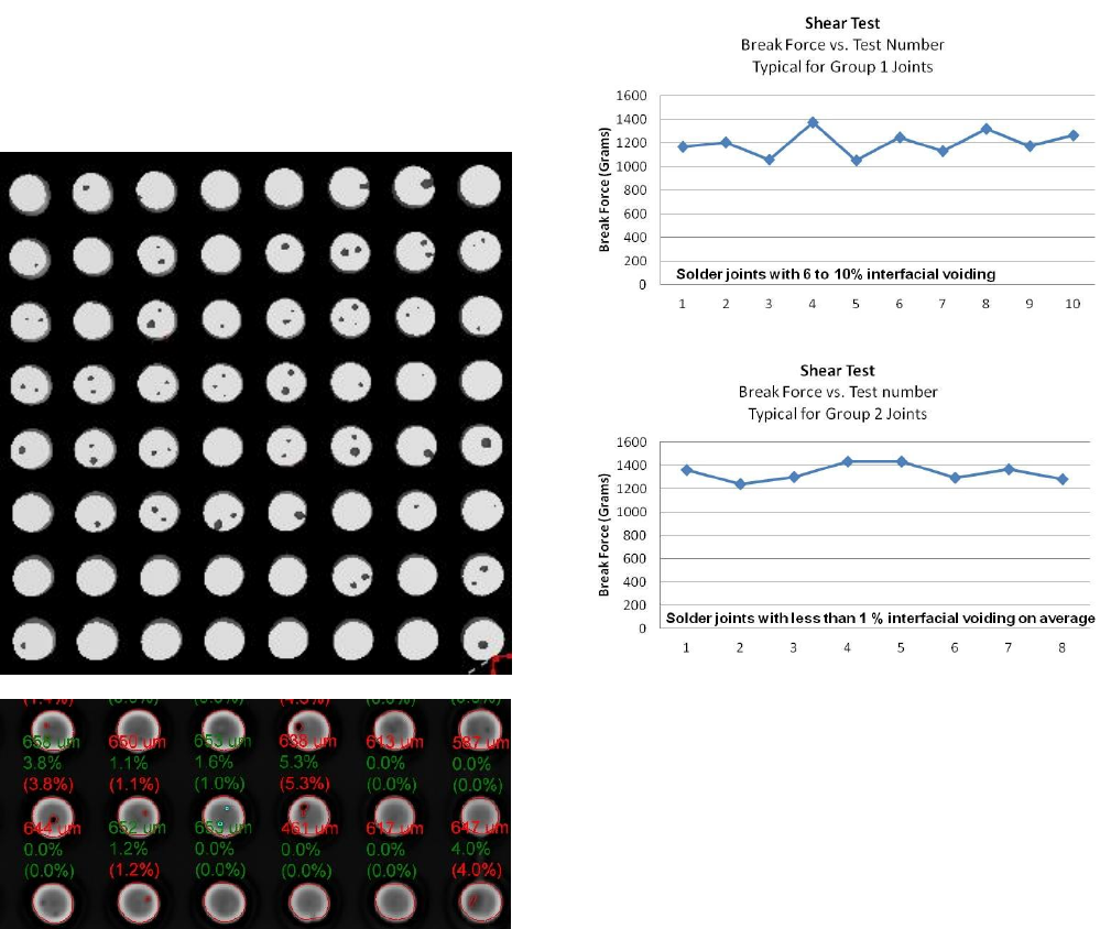
The shearing of the bonds was performed using a standard
Dage 4000 Plus bondtester. Contemporary bondtesters are
very versatile and accurate machines that perform a very
wide variety of mechanical tests both in a destructive and
non-destructive way. These include shear, pull, peel, and
also a large set of material tests like 3 and 4 point bend tests.
For certain testing conditions these machines can be
automated in order to achieve speed, productivity or better
accuracy.
Typical shear test results are shown on Figure 2. It is
obvious the joints in Group 2 (less than 1% interfacial
voiding on average) show more consistent and higher results
for break force compared to the joints in Group 1 (6% to
10% interfacial voiding).
(a)
(b)
Figure 2. Typical shear results for Groups 1 and 2 solder
joints. Group 2 joints (less than 1% voiding) show better
joint strength.
We observed two types of failure mechanisms due to the
shear testing – ductile and pad cratering, with the ductile
failure being significantly more proliferated. A ductile
failure is shown on Figure 3 and corresponds to a failure
that occurs in the solder bulk.