CASE-STUDY-IN-LINE-PARTICLE-SENSOR-8030170-REV_B.pdf
IN-LINE P ARTICLE SENSOR Improving Yields and T ool Uptime with In-Line Particle Sensor in Semiconductor Envir onments F ine par ticles can have disastr ous eects on semiconductor manufacturing, where devices ar e extre…
IN-LINE PARTICLE SENSOR
Improving Yields and Tool Uptime with In-Line Particle Sensor in
Semiconductor Environments
Fine particles can have disastrous eects on semiconductor manufacturing, where devices are extremely sensitive
and prone to damage by particulate contamination. Despite manufacturers’ best eorts to prevent contamination
through air ltering and recirculation methods, particles are still able to form inside process tools where they can
create defects and harm yields.
CyberOptics’ In-Line Particle Sensor™ (IPS™) provides a streamlined solution for particle detection and
maintenance. The IPS relieves pains of traditional monitoring methods while simultaneously increasing tool
uptime and improving yields.
Challenge
The three widely used methods for particle detection in photolithography
environments—benchtop and handheld particle counter, monitor reticles, and
in-situ monitor particle scanners—all have signicant drawbacks. It is often
impossible to reach all locations of interest using the benchtop and handheld
methods, while benchtop counters are also frequently incapable of following
the reticle path and monitor reticle scanning creates long delays before
delivering test results. The conventional approach is slow and takes tool time
which could instead be used to process product wafers—a missed opportunity
to improve yields.
Quickly identifying when and where airborne particles originate
is challenging with traditional methods, but it is critical to success.
Most monitoring relies on inspection with monitor wafers,
which are run through the process routinely or in response to
a contamination problem detected by downstream inspection
of product wafers. However, due to their intermittent nature,
conventional monitoring methods often miss contamination until
damage has already been done and is later detected downstream.
Manufacturers faced constant frustration attempting to locate precisely when and where airborne particles
originated while using imprecise traditional methodology. Managing contamination while maintaining
production speed was an uphill battle before the adoption of CyberOptics’ In-Line Particle Sensor (IPS) technology.
Continued >
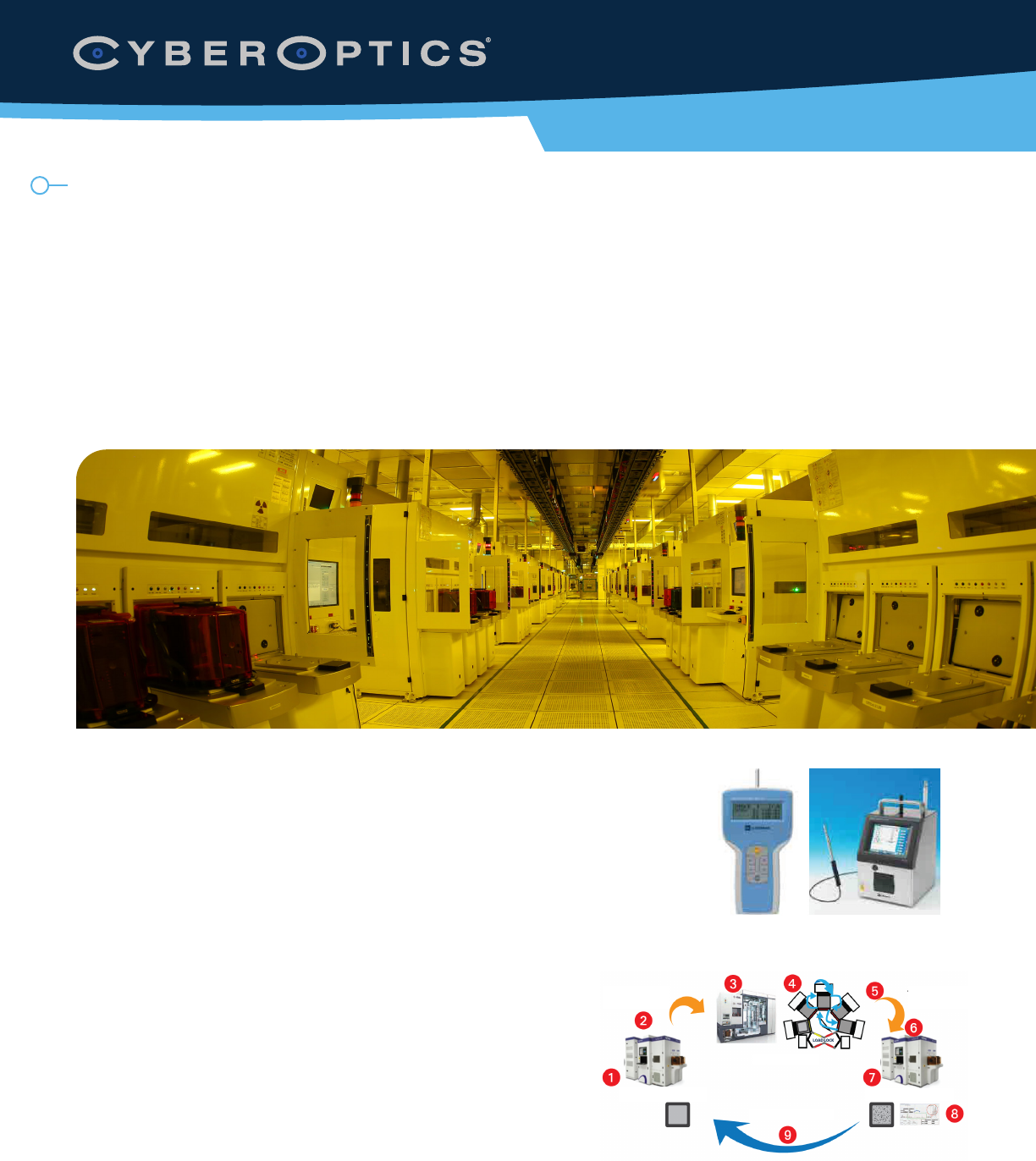
Handheld / Benchtop Counters
Monitor Reticle Scanning Process
Pre-measure
Load reticle
into scanner
Cycle Reticle
Repeat ?? times
Post-measure
Take reticle
into scanner
Contact CyberOptics today for more information
+1 800.366.9131 or +1 763.542.5000 | CSsales@cyberoptics.com | www.cyberoptics.com
Copyright © 2021. CyberOptics Corporation. All rights reserved. Specications subject to change without notice. 8030170 Rev B
For more information on CyberOptics products, services, or solutions, visit our website at www.cyberoptics.com.
Solution
CyberOptics’ In-Line Particle Sensor addresses these issues,
oering a solution informed by a thorough understanding of the
contamination and detection problems that process engineers
or operators face. IPS is an extension of CyberOptics’ Airborne
Particle Sensor™ (APS/APSRQ™) technology, which has been
recognized as the Best-Known Method (BKM) in fabs worldwide.
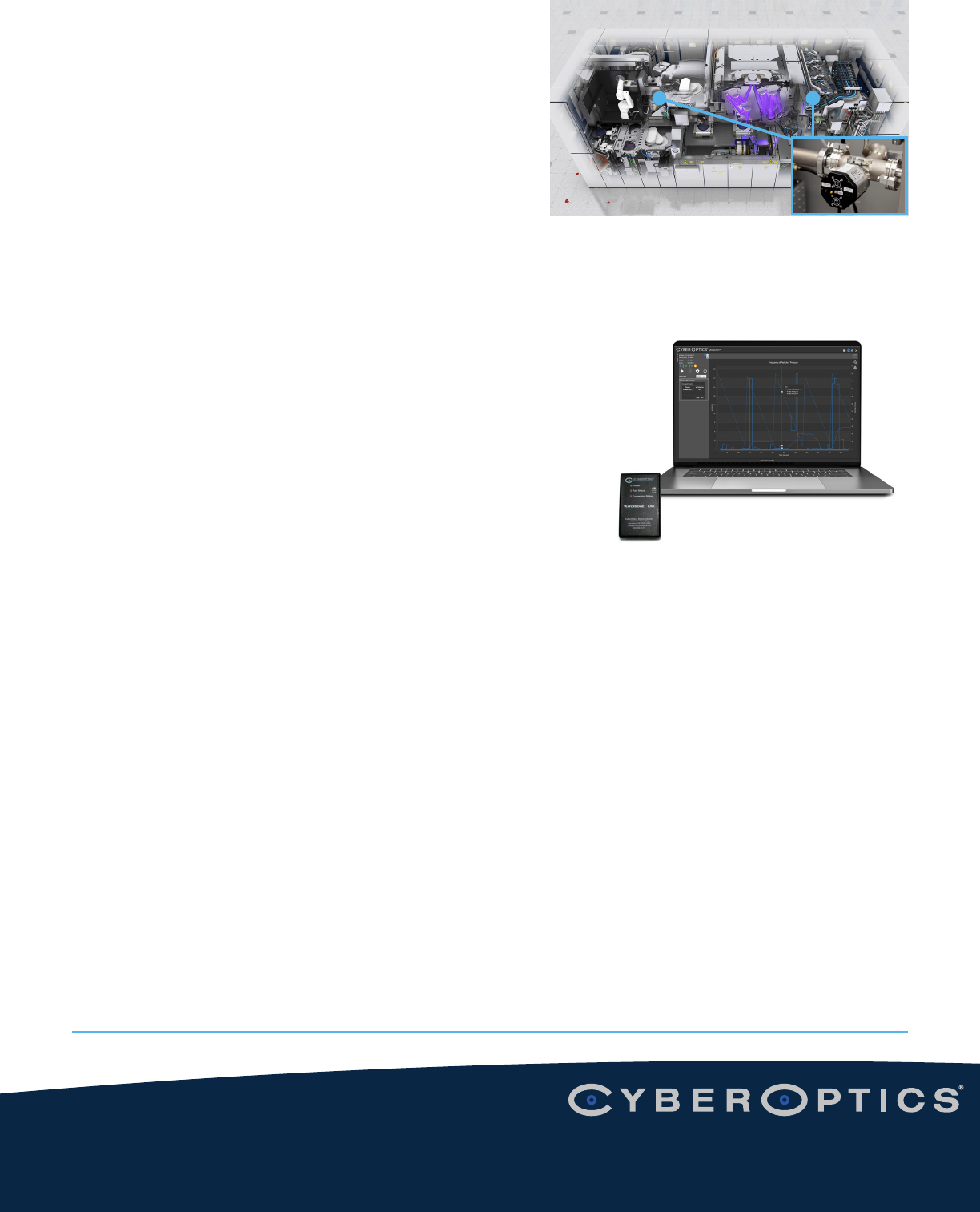
The IPS can be installed anywhere in the process chamber
exhaust line, where it utilizes a high-power blue laser to quickly
monitor, identify, and troubleshoot particles down to 0.1µm.
CyberOptics particle sensors can detect particle sources
precisely when and where they occur, thus dramatically improving tool-uptime and rst-pass wafer yields by
selectively servicing the portions of a tool causing particle generation. Unlike competitors’ products, the IPS works
continuously and in real time to deliver signicant productivity and cost benets.
By recording particle counts versus time, the IPS enables particle
generating events to be correlated with process events occurring inside
the tool. CyberSpectrum™ software displays real-time numerical and
graphical particle event data over time, including instantaneous and
average particle measurement results and accumulated particle counts.
The data is recorded to enable past and present comparison, as well as
comparison between tools. EUV customers, for instance, have shown a
clear correlation between IPS measurements and particle adder events.
Operators are spared the need to open tools in order to make particle
measurements.
In addition to CyberSpectrum software, the Software Development Kit (SDK) allows recorded data to be stored
in a network, thus eliminating the need for a designated data-storing PC. From this central location in the
cloud, any software can be utilized to analyze particle data. CyberOptics’ IPS is suitable for use in a wide range
of process sensitive applications including, but not limited to, Extreme Ultraviolet Lithography (EUV) processes,
semiconductor process equipment, vacuum chambers, 3D metal printing equipment, and equipment in
controlled environments.
Benet Summary
CyberOptics’ IPS helps producers maximize process yield and tool availability for contamination-free process
environments. IPS and wireless wafer and reticle format sensors detect particle sources precisely when and where
they form, with results available in real-time and conveniently stored for future analysis. Rapid results speed
detection of source contamination, shortening maintenance cycles as a result. Continuous monitoring eliminates
downtime and damage to in-progress work, ultimately improving yields while providing tremendous time and
cost saving benets.
About CyberOptics
CyberOptics Corporation is a leading global developer and manufacturer of high-precision 3D sensing technology solutions. CyberOptics’
sensors are used for inspection and metrology in the SMT and semiconductor capital equipment markets to signicantly improve yields
and productivity. By leveraging its leading edge technologies, the Company has strategically established itself as a global leader in high
precision 3D sensors, allowing CyberOptics to further increase its penetration of key vertical markets. Headquartered in Minneapolis,
Minnesota, CyberOptics conducts worldwide operations through its facilities in North America, Asia, and Europe.
IPS Locations: Supply and Exhaust Lines - Photo Illustration: ASML
CyberSpectrum Software