N5227B.pdf - 第89页
Find us at www. keysi ght.com Page 89 Figure 8 . Re c eiver B lock Diagram IF gate Anti - al i as fi l ter AD C Di gi t al F IR IF fi l ter Na rrowband fi l ter Ex ternal IF i nput A IF gate Anti-alias filter ADC Digital…
Find us at www.keysight.com Page 88
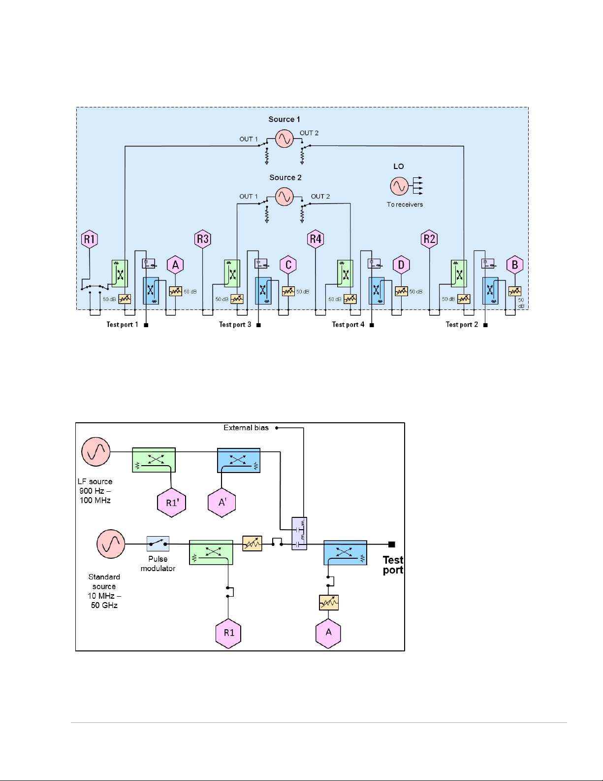
To base model, adds front-panel jumpers, R1 receiver switch, source and receiver attenuators
(extended power range), and bias-tees.
Figure 6. N5227B Option 419
The following LFE block diagram shows how the low-frequency hardware is configured for a single test
port. The other ports are configured similarly.
Figure 7. N5227B LFE Options
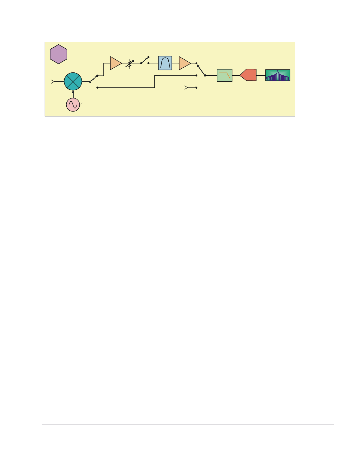
Find us at www.keysight.com Page 89
Figure 8. Receiver Block Diagram
IF gate
Anti-alias
filter
ADC
Digital FIR
IF filter
Narrowband filter
External
IF input
A
IF gate
Anti-alias
filter
ADC
Digital FIR
IF filter
Narrowband filter
External
IF input
AA

F
ind us at www.keysight.com Page 90
This information is subject to change without notice.
© Keysight Technologies 2017-2025
Print Date: August 1, 2025