DECAN_S1_Administrator′s_Guide(Eng_Ver1.5)_Print.pdf - 第143页
6-29 Board Definition Figure6.6 “Bad Mark Position” dialo g box (When the Posi tion Type is “None”) <Block Select> combo box For a Multi PCB The model selected from the “Board Definition” dialog box is selected…
6-28
Next Generation, Multi-Functional Placer DECAN S1 Administrator’s Guide
Memo Even though fiducial mark teaching is performed by changing the
workstation, all placement coordinates, fiducial mark coordinates and
the coordinates of various marks are always constant because the
relative distance from the origin is taught.
6.4. Bad Mark Setup
The ‘Bad Mark’ refers to the mark indicated on the PCB to show whether a small PCB in
the array PCB is good or defective. Placement is not performed on the small PCB
indicated defective.
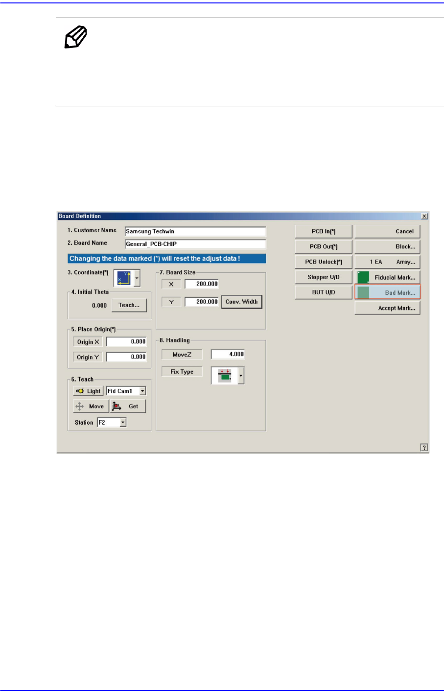
When this <Bad Mark…> button is clicked on, the following dialog box to edit bad mark
data is displayed.
6-29
Board Definition
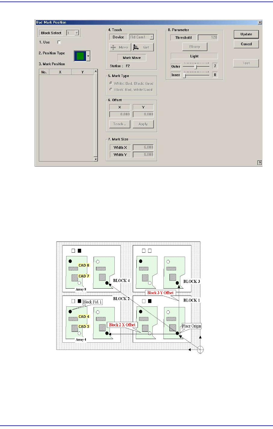
Figure6.6 “Bad Mark Position” dialog box (When the Position Type is “None”)
<Block Select> combo box
For a Multi PCB
The model selected from the “Board Definition” dialog box is selected
automatically and the corresponding combo box is disabled..
For a Block PCB
Select the model for which setup will be performed and set other items.
<1.Use> check box
Determines whether to use a bad mark.
<2. Position Type> combo box
Select a bad mark type. The bad marks that can be selected are as follow;
6-30
Next Generation, Multi-Functional Placer DECAN S1 Administrator’s Guide
None: Bad Mark.
Teach the bad mark on the first small PCB and determine the position of the bad
marks on each small PCB using the array offset that was already set up.
Set the bad mark offset to determine the bad mark positions automatically.
<3. Mark Position> group
If “None” is not selected in the <2. Position Type> combo box, data is created
according to the selected recognition type. The number of data generated is as follows;
When the <Position Type> is “Array”: 1
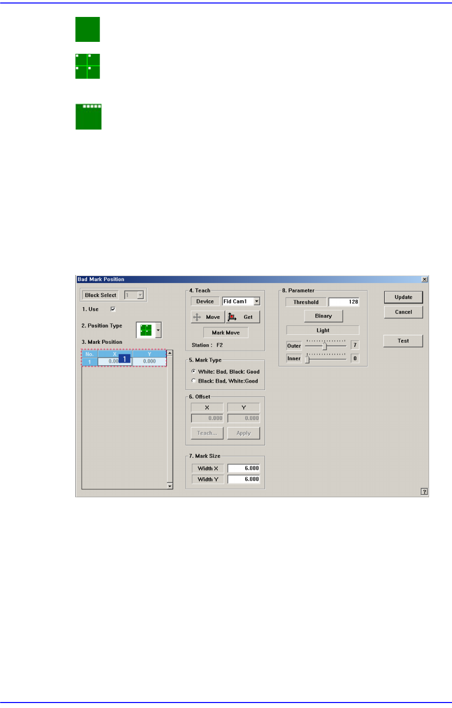
For example, when “Array” is selected in <2. Position Type> combo box, the
following dialog box is displayed. (When the number of Array PCBs is 4)
Figure6.7“Bad Mark Position” dialog box (When the Position Type is “Array”)
1:Grid Cell
<No> column
A serial number of bad mark data.
<X> column
The X position value of the bad mark.
<Y> column
The Y position value of the bad mark.
<4. Teach> group
Used for moving the fiducial camera to the assigned position of coordinates by