DECAN_S1_Administrator′s_Guide(Eng_Ver1.5)_Print.pdf - 第146页
6-32 Next Generation, Multi-Functional Plac er DECAN S1 Administrator’s Guide T each the first position of the bad mark. When the “Enter” key is pressed after teaching, the following screen is displayed. T each the posit…
6-31
Board Definition
rotating XY axis driving motor, or for obtaining the present coordinates of the fiducial
camera.
<Device> combo box
Select the Camera for checking Bad Mark. Selectable objects are as follows;
Fid Cam1/2: Select the fiducial camera.
<Move> button
Move the object selected in the <Device> combo box to the position of the
assigned coordinates. Before executing <Move> button, the cell in the grid
(Coordinates of the bad mark) corresponding to the desired position must be
clicked on with a mouse.
<Get> button
Obtain coordinates for XY, Z axis with reference to the object selected in the
<Device> combo box. At this time, the objects (Coordinates of the bad mark)
related with coordinates must first be clicked with the mouse before clicking on
the <Get> button.
<5. Mark Type> group
Select the color of bad mark. Available colors of bad marks are as follows.
Black: the mark looks darker than the surroundings.
White: the mark looks lighter than the surroundings.
<6. Offset> group
Used to set the offset value between bad marks automatically. It is enabled when
is selected in the <2. Position Type> combo box.
<X> edit box
Set the offset value of X.
<Y> edit box
Set the offset value of Y.
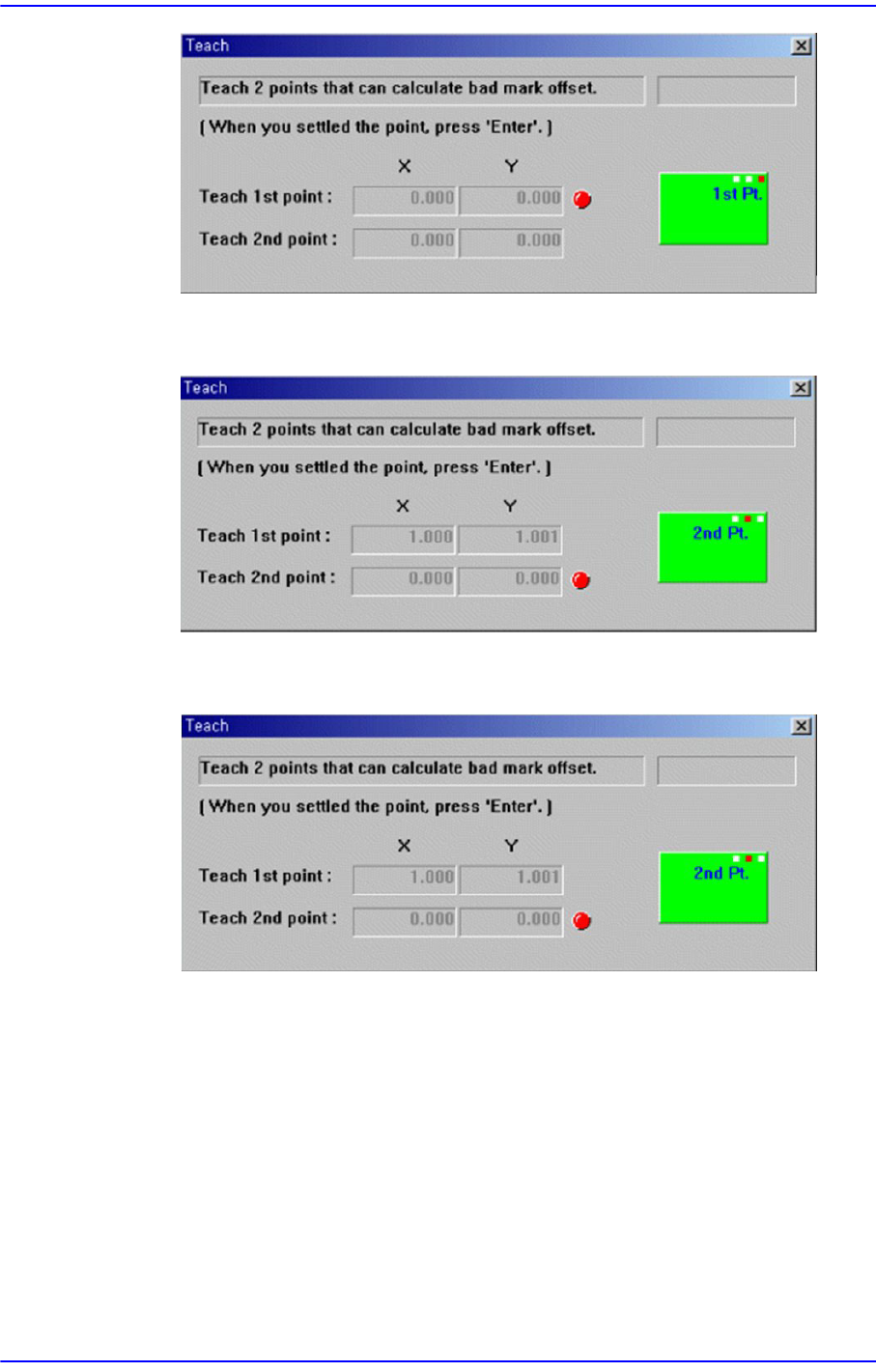
<Teach> button
Teach the offset value of bad mark. When this button is clicked on, the following
screens are displayed in succession.
6-32
Next Generation, Multi-Functional Placer DECAN S1 Administrator’s Guide
Teach the first position of the bad mark. When the “Enter” key is pressed after
teaching, the following screen is displayed.
Teach the position of the neighboring second bad mark. When the “Enter” key is
pressed after teaching, the following screen is displayed
Press the “Enter” key to complete the bad mark offset value teaching operation.
<Apply> button
Automatically creates the bad mark position data by using the offset value set
in this group.
<7. Mark Size> group
Set the area in which to search the bad mark. The main purpose of this feature is to
limit the search range for when there are forms similar to the mark near the mark such
that they can interfere with recognition on certain PCBs.
<Width X> edit box
Set the value of search range in X axis direction. In general, it is 6 mm..

6-33
Board Definition
<Width Y> edit box
Set the value of search range in Y axis direction. In general, it is 6 mm.
<8. Parameter> group
<Threshold> edit box
The image viewed through the SM Vision window is composed of each pixel.
Each pixel has a unique value between 0 and 255 according to the seen degree of
brightness. Here, ‘Threshold Value’ indicates the border value deciding whether
each pixel should be recognized in white or black. That is, setup the limitation for
deciding if the image pixel should be black or white when checking a bad mark.
For example, if <Bad Mark> is “Black” and the <Threshold> value is 100, then all
the values under 100 in the vision image are recognized as black, and if <Bad
Mark> is “White” and the <Threshold> value is 100, then all values over 100 are
recognized as white.
<Real Display/Binary> button
Shows the image seen through the SMVision in real display to which threshold is
not applied, or in the image (Binary) to which threshold is applied as recognized
by MMI.
<Light> group
Set the light value for bad mark inspection. In general it is 7, but adjust it
appropriately according to the condition of PCB and bad mark.
<Test> button
By using the registered mark information, tests the mark.. The accuracy of the
registered mark data can be verified. When the test is successful, the following
message box is displayed.
<OK> button
Saves the bad mark data and closes the “Bad Position” dialog box.
<Cancel> button
Closes the <Bad Position> dialog box without saving the bad mark data.
6.5. Accept Mark setup
The bad mark refers to the mark indicated on the PCB to show whether a small PCB in the
array PCB is good, acceptable or defective. The bad mark is indicated for defective PCBs
while the Accept Mark is not indicated for defective PCBs. However, in the case of the
Accept Mark, part placement is performed only in the PCB with the Accept Mark.
If no small PCB proves to be defective in the array PCB, it is not necessary to set the
Accept Mark, which will otherwise waste time.
In such cases, if setup is performed to use a bad mark but it is not used, the machine will