WaferTransportSolutionManual.pdf - 第113页
A3 DRAWINGS ELECTRICAL DRAWINGS Chapter Issue 1 Apr 11 Wafer Transport Solutio n 4.1 CHAPTER 4 A3 DRAWINGS ELECTRICAL DRA WINGS Electrical Description Drawing No. Sheets Issue State Circuit Thin Wafer Handling 200483 1 0…
INSTALLATION
EQUIPMENT INSTALLATION
3.36 Wafer Transport Solution Chapter Issue 1 Aug 11
Automatic Load In this mode of operation the CHAD Handler has wafers pre-loaded into the
system. The pallet is placed in the transport rails and wafers are loaded using
a robotic arm.
There are two CHAD Handlers:
• WaferMate 300-2 handling wafers from 200mm to 300mm diameter.
• WaferMate 200-3 handling wafers from 125mm to 200mm diameter.
Both systems provide a pair of front loading FOUP’s (Wafer Stacks). They
each have a four axis robotic arm which, dependent upon configuration,
provide wafer handling to one or two DEK printers.
1. Turn the mains isolator ON.
2. Wafers loaded in the FOUP's are picked out of the stack by the robotic arm.
3. The arm places the wafer into the aligner which spins it to detect the wafer
slot or notch position.
4. Once aligned, the wafers are loaded into pallets where they are fed into the
flux printer.
5. After printing, the pallet is fed back into the transfer station, through the
handler’s centre section and out to the opposite side transfer station, for
transfer to the ball placement printer.
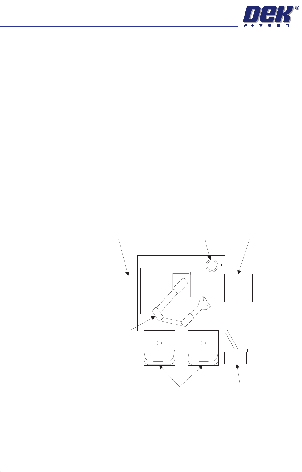
Figure 3-10 CHAD Handler Overview
6. The print quality can be monitored in the printer as part of its production
cycle. Software that is available to do this includes: Statistical Process
Control (SPC), 2D inspection™, HawkEye™ and HawkEye Bridging™.
External inspection systems include Sentinel™. Contact DEK for advice on
the best option for the application.
WaferMate Layout
FOUPs
MMI
Transfer Station
Aligner
Four-axis Robotic Arm
Transfer Station

A3 DRAWINGS
ELECTRICAL DRAWINGS
Chapter Issue 1 Apr 11 Wafer Transport Solution 4.1
CHAPTER 4 A3 DRAWINGS
ELECTRICAL DRAWINGS
Electrical
Description Drawing No. Sheets Issue State
Circuit Thin Wafer Handling 200483 1 02

A3 DRAWINGS
ELECTRICAL DRAWINGS
4.2 Wafer Transport Solution Chapter Issue 1 Apr 11