What is New in IPC-7351C.pdf - 第13页
PC B L ibr ar i es Pr e s ents : Wh at is N ew i n IPC- 7351C 3-Tie r Sil kscr ee n Outlines • T he r ec omm end ed guideli nes f or 3 -T i er l i ne width s and Sil k sc reen t o P ad G ap ar e il lus tr ated i n the pi…

PCB Libraries Presents:
What is New in IPC-7351C
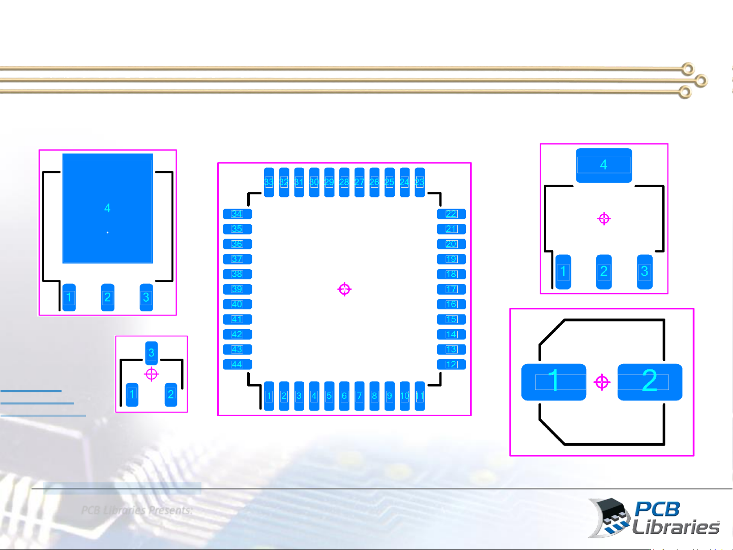
1. No silkscreen outline under the component body; these get covered up
during assembly and don’t provide any useful purpose (waste of good ink)
2. Silkscreen outlines visible after assembly process and provide a functional
use as alignment marking for assembly registration accuracy
3. Silkscreen outlines should be inside placement courtyard
4. Silkscreen outlines should be mapped to the Maximum Component Body
with one exception, the Silkscreen to Pad spacing rule “overrides” the
Component Body Mapping
5. Silkscreen outlines should map the component body and not go around
pads. Excess silkscreen outlines should be avoided to make room for ref
des locations. Silkscreen outlines should perform a “hatch” outline along
the component package body.
6. Pin 1 is identified by extending the silkscreen along Pin 1 length of pads
when component leads extend outward. Bottom only terminals Pin 1 is
identified by a missing line.
Silkscreen Outline Guidelines
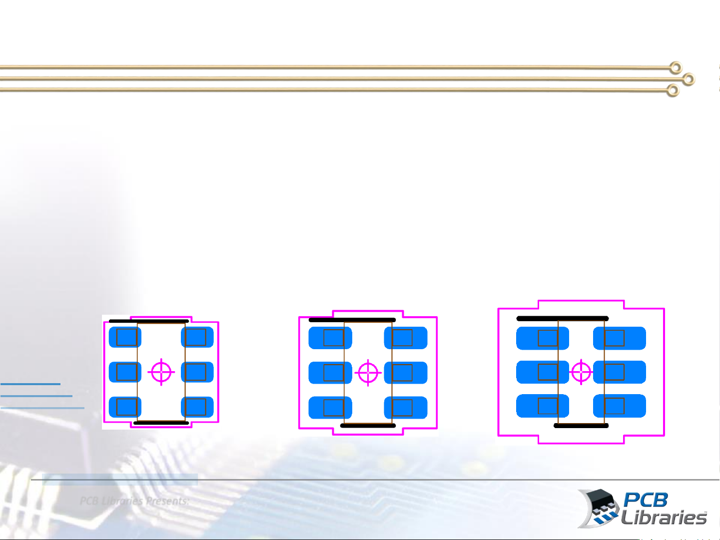
PCB Libraries Presents:
What is New in IPC-7351C
3-Tier Silkscreen Outlines
• The recommended guidelines for 3-Tier line widths and
Silkscreen to Pad Gap are illustrated in the pictures below
representing a SOT23-6 component package
• The Silkscreen to Pad Clearance is the same as the Line Width
Least Density Level
0.10 mm Line Width
Nominal Density Level
0.12 mm Line Width
Most Density Level
0.15 mm Line Width
PCB Libraries Presents:
What is New in IPC-7351C
IPC-7351B Rectangular Courtyards
The recommended courtyard outline line widths are 0.05 mm or 0.01 mm