PARMI_Xceed MICRO_Eng
MICRO ‘Xceed MICRO’ is a precise and high speed 2D & 3D AOI machine. It is optimized for inspections required in PCB, lead-frame, FC, and SiP assembly process such as die attach, cu clip attach, underfill, solder pas…
MICRO
‘Xceed MICRO’ is a precise and high speed 2D & 3D AOI machine. It is optimized for
inspections required in PCB, lead-frame, FC, and SiP assembly process such as die
attach, cu clip attach, underfill, solder paste and ball attach. ‘Xceed MICRO’ delivers
precise 2D inspection capability and at the same time it performs high speed 3D
inspections (Height, Tilt, Lift, and Volume) with its highly focused laser beam.
Additionally, ‘Xceed MICRO’ is the only machine capable of inspecting foreign
material/contamination and warpage on the die surface, metal lead frame, and
PCB substrates simultaneously.
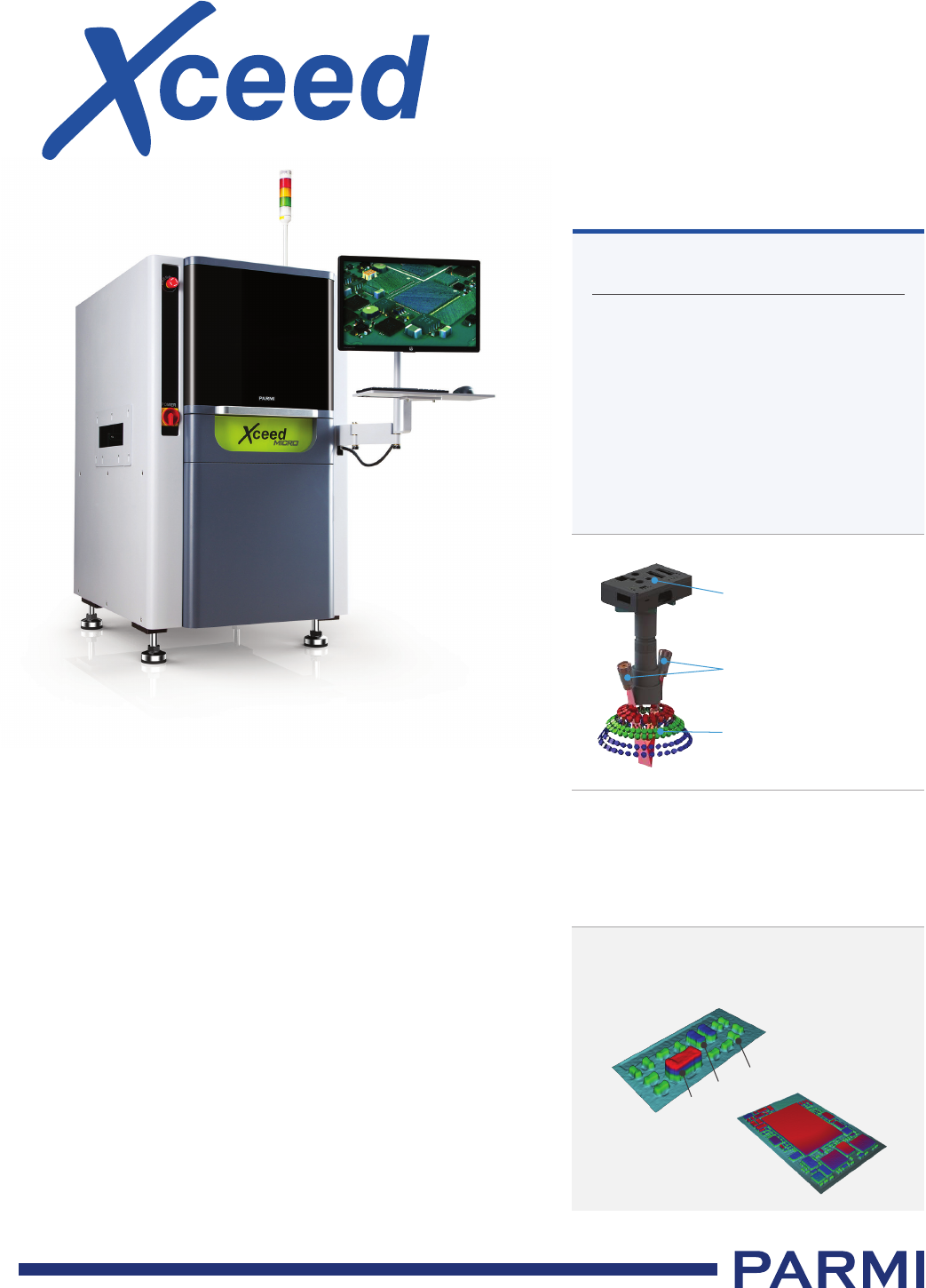
Our patented 2D & 3D vision optics unit (TRSC) creates 2D color images by using a
3 channel RGB LED illumination system and 3D data with 2 channel laser sheet
beam. The entire inspection is completed with only a single scan. It is possible to
apply either 3.5µm or 7.0µm resolution vision unit selectively based on the required
inspection application or measurement accuracy. PARMI’s exclusive laser scan
technology can accurately inspect highly specular components and materials such
as bare die, IPD, and underfill fillet while other conventional AOI system reflect light
away making inspection difficult. Since 3D data is created at a speed more than
several hundred times faster than the laser pointer method, it is possible to
perform 100% inspection and eliminate random sample inspection. PARMI also
guarantees extremely low ‘Escape’ and ‘False call’ rates through outstanding
laser optical triangulation method.
The required time to make a single teaching program with the user friendly
designed UI (User Interface) and advanced intelligent algorithm is typically less
than 30 minutes. Moreover, various software tools such as e-Map, SPC (Statistical
Process Control), operator 2
nd
verification, remote control and monitoring, and
offline software are available.
Key Features
•
Extremely fast laser scan 2D & 3D AOI
•
Highly focused 2 channel laser for 3D data
generation
•
3D laser can inspect highly specular surfaces
(Bare die, IPD, Die Attach, and Underfill fillet)
•
High bandwidth on a broad range of colors,
surface roughness, and materials
•
Virtually zero escape & false call rates
•
Specular Die, IPD, Tiny Chip (0201~ : metric)
• Tilt, Dimension, Misalignment, Soldering, Bridge,
Crack, FM/Contamination on substrate
SiP (System in Package)
0603
0201
0402
Ultra Fast 2D & 3D Sensor
Signal Processing by FPGA
Shadow Free Dual Laser : 3D
7 Channel LED : Color 2D
Ultra-Precision Laser Scan 3D AOI for
Semiconductor Packaging
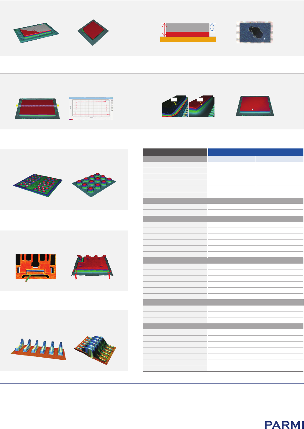
Die Attach
• BLT (Bond Line Thickness)
• Die Tilt, Misalignment, Chipping, Crack
• Epoxy Coverage, Fillet Height and Runout measurement
• FM/Contamination, RBO (Resin Bleed Out)
Die ContaminationBLT= Die Height(H) – Die Thickness(D)Die Tilt Die Chipping
※
Specifications in this catalog are subjected to change without notice for quality improvement. Rev.1
Specifications
Shadow Free Dual Laser Optical Triangulation
4M Image Sensor / Telecentric Lens
R.G.B LED 3 Stage Lightings
3.5 × 3.5 7 × 7
3.75
5
15
15
3 sigma < 3µm
2µm
50 × 50
410 × 350
0.08 ~ 5
2
2.5 / 3.3
30 / 15
850 × 1,205 × 1,525
730
860 ~ 970
300 ~ 800
Left to Right, Right to Left (Factory Setting)
Auto
i7-7800X or above
Teaching Program
SPC&Process Monitoring
Verification Program
24" Monitor
Windows 7 or above
Barcode(1D/2D) Recognition
SPCworksAOI, xNetHub
AOIworks
(Option) Offline Teaching Program
Veriworks
AOIManager, AOIDBManager
ePM (Gerber, BOM, Cad)
Built in AOIworks
AOIworks Offline
TRSC
-
×2 TRSC
-
×2
Xceed MICRO
Measuring Principle
Camera
Illumination
Scan Speed (sq.cm/sec)
X-Y Resolution (µm)
Max. Component Height (mm)
Height Repeatability
Height Accuracy
Min. Size (mm)
Max. Size (mm)
Thickness (mm)
Max. Weight (kg)
Top/Bottom Clearance (mm)
W×D×H (mm)
Weight (kg)
Conveyor Speed Range (mm/sec)
Conveyor Width Adjusting
CPU
Operating System
Display
Vision Module
Model
Top/Bottom Edge Clearance (mm)
Conveyor Height (mm)
Inspection Program
System Diagnosis
Panel Flow Direction
IGBT
•
Die Position, Tilt, Contamination
•
Wire loop Height, Misalignment, Bridge, Stitch
PARMI USA Inc. East (Boston)
•
E-mail : jbashe@parmiusa.com
•
Tel : +1.508.485.8120
PARMI USA Inc. West (San Diego)
•
E-mail : fsilva@parmiusa.com
•
Tel : +1.858.683.0225
PARMI China (Dongguan)
•
E-mail : jordan@parmi.com
•
Tel : +86.769.8150.1199
PARMI East China (Suzhou)
•
E-mail : yc@parmi.com
•
Tel : +86.512.6280.5996
PARMI Japan (Tokyo)
•
E-mail : parmijapan@parmi.com
•
Tel : +81.3.6264.8744
PARMI Europe GmbH (Germany)
•
E-mail : parmieurope@parmi.com
•
Tel : +49.6102.799.098.0
PARMI HQ
•
Address : 32-18, Yuseong-daero
1596beon-gil, Yuseong-gu, Daejeon,
34054, Korea
•
E-mail : parmi@parmi.com
•
Tel : +82.42.478.9900
•
Webpage : www.parmi.com
Solder paste and Bump
• Height, Area, Volume, Misalignment, Bridge, Coplanarity
• Substrate Warpage, FM/Contamination
Solder paste Solder ball
Cu Clip on die
• Die Misalignment, Tilt, BLT, Fillet Coverage and Height
• Cu Clip Height, Tilt, Warpage, Misalignment, Fillet Coverage
and Height
Solder Fillet Joint Misalignment
Underfill
• Die and Package Tilt, Misalignment, Chipping, Crack • UF Coverage, Fillet Height and Runout measurement
• FM/Contamination, RBO (Resin Bleed Out)
Cross section of Package & Underfill Fillet Height Foreign material
Fillet Fillet
H
D
Solder or Epoxy
Die
Performance
Panel Dimension
System Dimension
Computer & Console
Software