F5HM Circuit Diagrams.pdf - 第106页
3 Options Circui t Diagrams 106 0034533 3-010101 LD4 Cable: d istributo r , PCB barco de - MC Sheet Urspr. Ers. f. Ers . d. SIEMENS AG Sh. The arrow al ways points to the top left-hand c orner of the lab eling fiel d. In…
3 Options Circuit Diagrams 105
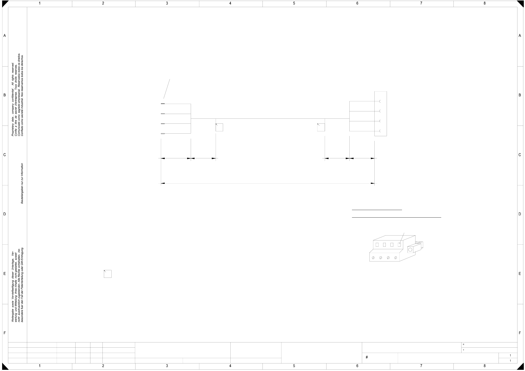
00345332-010101LD4 Cable: power supply, PCB barcode
Blatt
Urspr. Ers. f. Ers. d.
SIEMENS AG
Bl.
The arrow always points to the top left-hand corner of the labeling field.
Information on the printing and appearance of the
labels is given in the labeling guidelines for made-up cables
specified in the parts list.
Zustand
01.
01.
01.
Aenderung
Function status
Doc. status
Product status
04.12.98
04.12.98
04.12.98
Datum Name
Tek
Tek
Tek Datum
Gepr.
Bearb.
26.10.1998
Fux
Norm
SMD-Placement System Siplace
1
1
W1
To
Cable ferrules
3
I/O panel A2
(GND)
I/O panel A2
Phoenix COMBICON FRONT-MC plug
432
PCB barcode power supply
at X212/4
at X2kc:7
2
Pin assignment of the
4
30mm
To
l = 5 m ± 0,05 m / 8 x 0,34 mm²
terminal panel (left-hand side)
X6
PCB barcode distribution board
50mm50mm1000mm
wh+br
gn+ye
gr+pk
bl+rd
wh+br
gn+ye
gr+pk
bl+rd
at X212/3
at X2kc:4
(+24V)
Cable:
00345332-010101LD4
0,75 mm²
PL EA1 E2
3 Options Circuit Diagrams 106
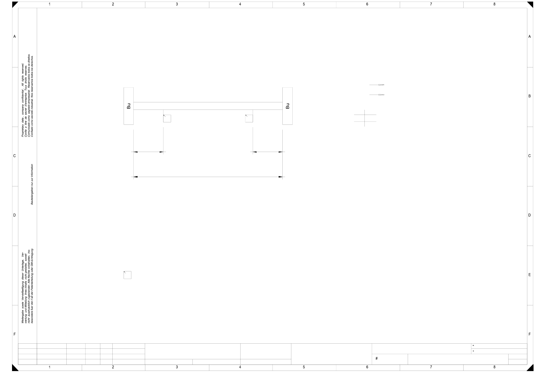
00345333-010101LD4 Cable: distributor, PCB barcode - MC
Sheet
Urspr. Ers. f. Ers. d.
SIEMENS AG
Sh.
The arrow always points to the top left-hand corner of the labeling field.
Information on the printing and appearance of the labels
is given in the labeling guidelines for made-up cables
specified in the parts list.
Sub-D socket, 9-pin
W1
X5 X*sa
l = 5m
70mm 70mm
PCB barcode - MC distribution board
X5
X*sa
Sub-D socket, 9-pin
PL EA1 E2
00345333-010101LD4
Cable :
Zustand
01.
01.
01.
Aenderung
Function status
Doc. status
Product status
22.02.99
04.12.98
04.12.98
Datum Name
Tek
Tek
Tek Datum
Gepr.
Bearb.
26.10.1998
Fux
Norm
SMD-Placement System Siplace
1
1
X*sa
X8sa
X6saM44
M54
4 Printed Circuit Boards 107
4 Printed Circuit Boards
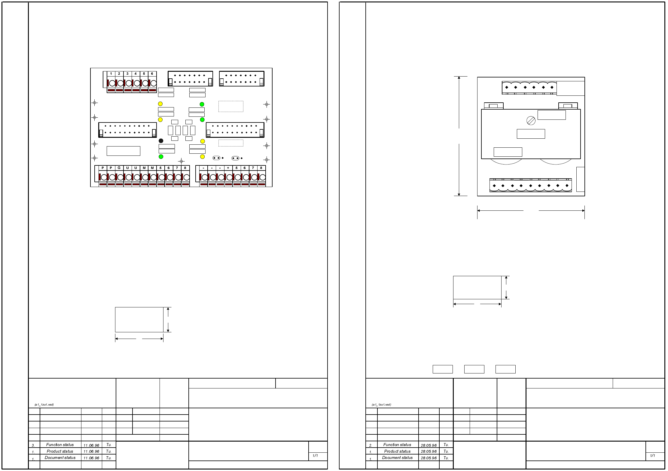
00200034-030101ND4 Optical decoupling unit
00300167-020101ND4 Rectifier board, 30 V
28.05.1996
28.05.1996
00300167-020101ND4
SIEMENS
Aktiengesellschaft
AUT 5 BPB BS1
Datum
Bearb.
Gepr.
Norm
Name
Dateiname:
Zust.
Mitteilung
Datum
Name
(Materialnummer)
Format A4
Mat.-Nr.: FS ES US S/F
Blatt
Maßstab
Weitergabe sowie Vervielfältigung dieser Unterlage, Verwertung und Mitteilung
ihres Inhaltes nicht gestattet, soweit nicht ausdrücklich zugestanden.
Zuwiderhandlungen verpflichten zu Schadenersatz. Alle Rechte für den Fall
der Patenterteilung oder GM-Eintragung vorbehalten.
Copying of this document, and giving it to others and the use or communication
of the contents thereof, are forbidden without express authority. Offenders are
liable to the payment of damages. All rights are reserved in the event of the
grant of a patent or the registration of the utility model or design.
00300167.21N
65 mm
72 mm
V1 V2
X1
X2
A
A1
X1ra
X2ra
1
1
X1raA1 X2ra
Siemens AUT5
00300167-02
AA-BBBB-CCCC
15
10
B
SMD Placement System Siplace
Rectifier board 30V
1 : Assembly designation
Assembly inscription acc. to recommendation VA-F-510-001
Labels: size approx. 5x12mm, font size 3 mm
or engrave on the heat sink.
2 : Plug designation
The following labels have to be stuck on:
A: Identification label
B: Inspection label
Assembly inscription acc. to recommendation VA-F-510-001
font size 1,5 mm, mat. Scotchcal 3698-E ( color A1 Ral 9006 )
AA = manufacturer/location acc. to SN 37040
BBBB = date (year/month/day) acc. to SN 01007
CCCC = numeral
Product inspection certification acc. to recommendation VA Q 509-001
11.06.1996
11.06.1996
00200034-030101ND4
Siemens
Aktiengesellschaft
AUT 5 BPB BS1
Datum
Bearb.
Gepr.
Norm
Name
Dateiname:
Zust.
Mitteilung
Datum
Name
(Materialnummer)
Format A4
Mat.-Nr.: FS ES US S/F
Blatt
Maßstab
Weitergabe sowie Vervielfältigung dieser Unterlage, Verwertung und Mitteilung
ihres Inhaltes nicht gestattet, soweit nicht ausdrücklich zugestanden.
Zuwiderhandlungen verpflichten zu Schadenersatz. Alle Rechte für den Fall
der Patenterteilung oder GM-Eintragung vorbehalten.
Copying of this document, and giving it to others and the use or communication
of the contents thereof, are forbidden without express authority. Offenders are
liable to the payment of damages. All rights are reserved in the event of the
grant of a patent or the registration of the utility model or design.
R3
U1
R2
R4
R6
R5
R9
R10
V2
V1
X2
V6
R8
R7
R11
R12
V4
V3
V7
V8
R1
U2
U3
U4
C1 C3
C2 C4
MP1
MP2
MP3
MP4
MP5
MP6
MP7
MP8
V5
X1
X7
X4
X3
X6X5
JP1 JP2
1 2 3 1 2 3
00200034.31N
B
MP9
A
K1
Zeichn.Nr.alt: 1710460 Y0020 000 02
Assembly inscription according to recommendation VA-F-510-001
Font size 1 mm, material Scotchcal 3698-E ( color A1 Ral 9006 )
AA = manufacturer/location acc. to SN 37040
BBBB = date (year/month/day) acc. to SN 01007
CCCC = numeral
Product inspection certification acc. to recommendation VA Q 509-001
The following labels have to be stuck on:
A : Identification label
B : Inspection label
Note: Set jumpers JP1 and JP2 to left position (1-2) when delivering !
Siemens AUT 5
00200034-03
AA-BBBB-CCCC
20
10
SMD Placement System Siplace
Optical decoupling unit