F5HM Circuit Diagrams.pdf - 第89页
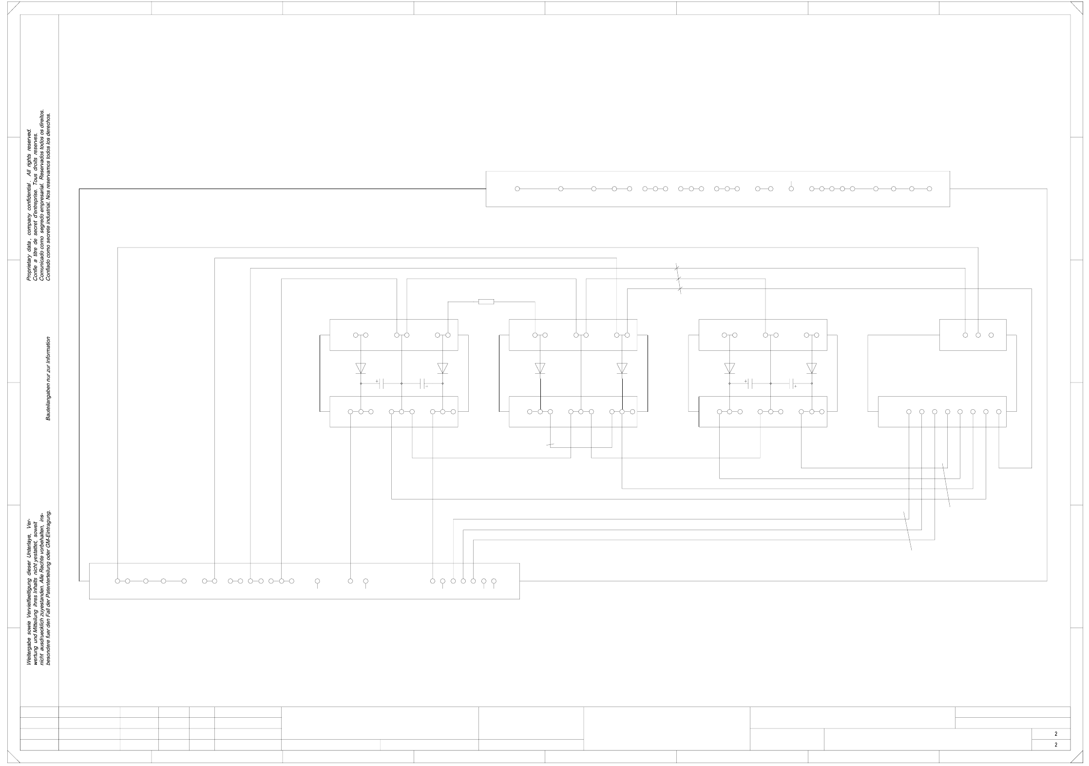
2 Circuit Diagr ams 89 0033734 2-030101TD3 T ermin al panel, r ighthand sid e L2 L3 X206 6 4 A2 10 220mm X X 1 6 X END X1rc X1r b X2re 7 X X X N N N N N 3 D C 15 Cabl e duc t 65x30 l=335mm L2 X 5 8 E F F 2 X 10 X206 L1 L…
2 Circuit Diagrams 88
00337342-030101LD3 Voltage rectification, prewiring, terminal panel, righthand side (Sh. 2 of 2)
SMD-Placement System Siplace S23
Product status
Doc. status
Function status
(terminal panel, righthand side)
=
Datum
Gepr.
Norm
Bearb.
Blatt
Upkpr. Epk. f. Epk. d.NameDatumAenderungZustand
SIEMENS AG
Bl.
+
Leh
Leh
Leh
01
01
01
05.02.98
05.02.98
05.02.98
05.02.98
Tuth
#
Voltage rectification prewiring
00337342-010101LD3
89
(rc) (rd)
56
123 456 78
10 10 19 11
1
(rb)
X1
1
987116
X1
10 4
12 34 56
12
(+24V)
br
gr
ye
wh
(re)
X206
X207
345678 67
pk
1mm²
1mm²
gn
gn
wh
9
X2
X2
A2 A3 A4 A5
10
bk bk1mm²
wh
672
23456
X1
23
wh
1mm²
(K1)
(K2)
(+24V)
bl/bk
bl/bk
5
9 123 45
(K2)
bk
1,5mm²bk
bk
pk
br
6L+ unswitched
X2
X1
12 34
2L+
2L+
678
12345
wh
18 18 8 8 9 9
2L-
16
78
A
B
wh
wh
345
12
X1
1
wh
wh
bl/bk
gr
2,5mm²wh
(K1)
PE PEPEPEPE
bk
0,5mm²
gr
+7L switched
2L+/5L+
ye2L+/5L+
2L-
45
PEPENNNN 42
6
1mm²
gn 1mm² gn
15
35111 433
1mm²
gr
wh
wh
1mm²
A
22
171413
C
D
E
FF
E
D
C
B
bl/bk
bl/bk
bl/bk
bk
1,5mm²bk
N
123
PEPE
4,7 Ohm / 5W
R1
21
PL EA1 E5
2 Circuit Diagrams 89
00337342-030101TD3 Terminal panel, righthand side
L2
L3
X206
6
4
A2
10
220mm
X
X
1
6
X
END
X1rcX1rb
X2re
7
X
XX
N
N
N
N
N
3
D
C
15
Cable duct 65x30 l=335mm
L2
X
5 8
E
FF
2
X
10
X206
L1
L1
L1
L2
L2
Cable duct 65x46 l=155mm
7
345
130mm
X
XX
11
12
A
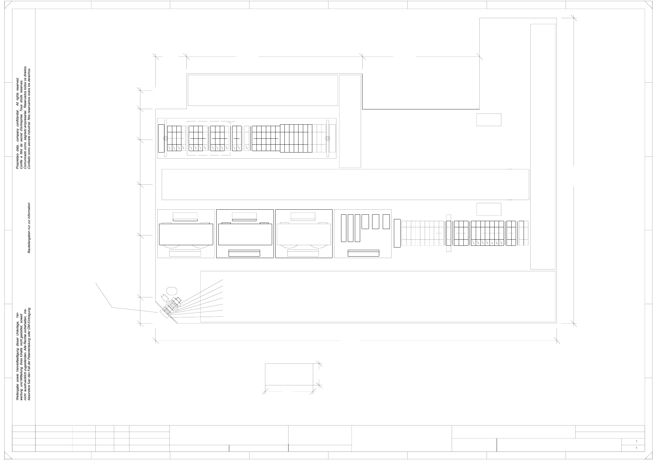
Note: X means that one lug must be knocked out
420mm
8
9
N
5
116mm
4
PE
PE
PE
PE
X
10
Cable duct 65x66 l=460mm
Note: X means that one lug must be knocket out
8
8
16
Cable duct 65x30
E
B
2
C
D
17
18
18
19
6
35mm
190mm
252mm
L3
L3
L3
13
14
B
X2rb
6
5
500mm
12
l=120mm
A
7
L1
4
X
XX
Leh
Leh
03
01
01
21.10.98
12.03.98
08.06.98
21.10.98
Tuth
#
Terminal panel, righthand side
00337342-030101TD3
Cable duct 65x46 l=430mm
1
X207
A
PE
PE
PE
PE
PE
PL EA1 E5
Leh
Contact washer SN 70093
Nut DIN 439
Annular cable lug
Washer DIN 125
Split washer DIN 7980
Nut DIN 439
=
Datum
Gepr.
Norm
Bearb.
Blatt
Urspr. Ers. f. Ers. d.NameDatumAenderungZustand
SIEMENS AG
Bl.
+
D:
XX
D
B
55mm
A5
A4A3
C
acc. to BV 00343603, Sh.2
Ground connection
PE
X
X
270mm
X1rd
XX
315mm
0mm
X
Please note:
- Jumper X207 13-14-15-16-17 should be moved to
X207 11-12-13-14-15 when the X and Y axes
are started up for the first time.
This will switch from 1L+ (100V) to 4L+ (8V),
thus reducing the risk of a head crash.
SIEMENS PLEA 1
00337342-03
AA-BBBB-CCCC
40
20
X2rdX2rc
3
X
SMD-Placement System Siplace S23
Product status
Doc. status
Function status
The following labels have to be applied:
A: Identification label
Space for voltage label from NAFTA lable set (for USA only)
C: Ground label
B: Inspection label
Identification: Testing engineer, month, year
BBBB = Date (year/month/day) acc. to SN 01007
AA = Manufacturer/location acc. to SN 37040
CCCC = Series number
Font size 2.5mm Material Scotchcal 3698-E (Color A1 RAL 9006)
Assembly inscription acc. to guideline VA - F - 510 - 001
Screw
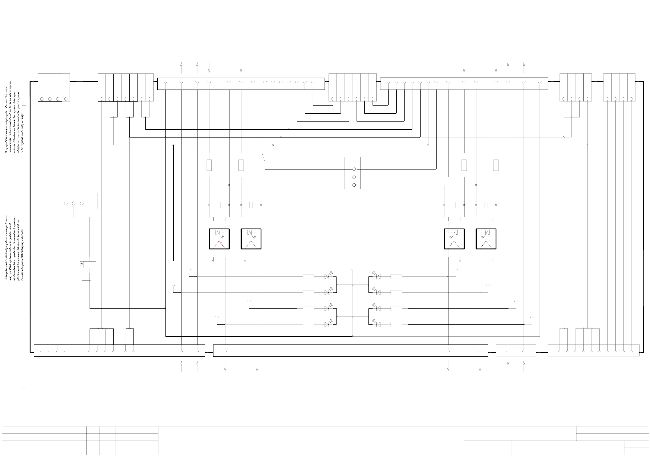
2 Circuit Diagrams 90
00200034-030101LD3 Signal decoupling unit
34
12
+-
+-
+-
+-
34
21
34
21
Name Norm
Beab.
Urspr./Ers.f./Ers.d.
Bl.
Bl.Stromlaufplan/Circuit diagramDatumAenderungZustand
Datum
Gepr.
1816151413121110987654321 17
CAD-Datei :
Mat.-Nr. :
SIEMENS
AUT 5
Product status
Doc. status
SMD Placement System Siplace 80S
1
1
29.10.1990
Tekin
Optical decoupling
unit
1. Tu.
14.06.96
GND 24V
X1 9
K1
13
6
9
1 2 3
JP2
X5 8
1413
GND 24V
GND 24V
10 11 12
5
6
7
X5
X5
X5
GND 24V
Received
Permission
151413X3
65
Permission
Received
MP2
MP1
1K5 1,1W
R1
0,1uF
C1
Request
GND n-1
19 20
Request
U1
MP4
GND 24V
11
loop
K1
1
7
Fault signal
12
1K5 1,1W
R2
0,1uF
C2
Transferred
18
previous station
To
U2
6
Transferred
2K7
R8
2K7
R7
MP3
2K7
R5
2K7
R6
Permission
Received
Transferred
Request
+24VDC
Spare
Spare
Spare
1098
+30VDC unswitched
+24VDC
123
GND 24V
X7
X7
X7
X7
X7
1
2
3
4
5
6X7
Spare
Spare
Spare
Spare
Spare
Spare
1
2
3
JP1
MP9
V2
+-
V1
+-
V3
+-
V4
+-
ye
ye
gn
gn
gn
gn
ye
ye
V8
V7
V5
V6
Spare
Spare
Spare
9810X4
+24VDC
GND 24V
+30VDC unswitched
564
2K7
R11
2K7
R12
2K7
R10
2K7
R9
Permission
Transferred
Request
Received
11
Fault signal
12
loop
following station
To
1K5 1,1W
R3
0,1uF
C3
Permission
15
7
Permission
U3
MP5
GND 24V
1K5 1,1W
R4
0,1uF
C4
Received
GND n+1
1413
8
Received
U4
MP6
Request
GND 24V
Transferred
18 19 20
7
Transferred
Request
MP7
MP8
X1 8X2 5
Tu.
14.06.96
3.
Output 1
Output 2
Output 3
Output 4Output 4
Output 3
Output 2
Output 1
6
7
8
X6
X6
X6
5 X6
12111091234
+ X6
+24VDC
+24VDC
+24VDC
+24VDC
Input 1
Input 2
Input 3
Input 4 Input 4
Input 3
Input 2
Input 1
+24VDC
U
U
X5
X5
P
P
M
X5
X5
X5
M X5
+30VDC unswitched
+30VDC unswitched
GND 24V
GND 24V
+24VDC
+24VDC
G X5
1234
GND 24V
GND 24V
GND 24VX6
X6
X6 -
-
-
GND 24V
GND 24V
X2 13 14
+30VDC switched
+30VDC switched
+30VDC switched
+30VDC switched
+30VDC switched
00200034-030101LD3
1.
Tu.
14.06.96
Function status
00200034
00200034-03
34
12