三星规格书.pdf - 第21页
Multilayer Ceramic Capacitor - 20 - ■ CHARACTERISTIC GRAPH 0 50 100 100 0 100 00 0 10 -10 -20 -30 Time(Hr) Δ C % C0G X7R Y5V ▶ CAPACITANCE CHANGE - AGING -60 140 0 -20 20 60 100 Temperature( ℃ ) Δ C % 0 5 -5 -10 10 C0G U…
Multilayer Ceramic Capacitor
- 19 -
NO
ITEM PERFORMANCE TEST CONDITION
16
HIGH
TEMPERATURE
RESISTANCE
APPEARANCE NO MECHANICAL DAMAGE SHALL OCCUR APPLIED VOLTAGE :
200% OF RATED VOLTAGE
TEST TIME : 1000 +48/-0 Hr.
CURRENT APPLIED : 50
㎃
MAX.
<INITIAL MEASUREMENT>
CLASS
Ⅱ
SHOULD BE MEASURED INITIAL
VALUE AFTER BE HEAT-TREATED FOR 1 HR
IN 150
℃
+0/-10
℃
AND BE LEFT FOR 48
±
4HR
AT ROOM TEMPERATURE.
<LATTER MEASUREMENT>
CLASS
Ⅰ
SHOULD BE MEASURED AFTER LEFT
FOR 24
±
2 HRS IN ROOM TEMPERATURE AND
HUMIDITY.
CLASS
Ⅱ
SHOULD BE MEASURED LATTER
VALUE AFTER BE HEAT-TREATED FOR 1 HR
IN 150
℃
+0/-10
℃
AND BE LEFT FOR 48
±
4HR
AT ROOM TEMPERATURE.
(TWICE OF RATED VOLTAGE WILL BE APPLIED
TO ALL SERIES BUT ABOVE)
** HOWEVER, A/B
는
1005 C
≥
0.22
㎌
CAPACITANCE
CHARACTERISTIC CAP. CHANGE
CLASS
Ⅰ
WITHIN
±
3% OR
±
0.3
㎊
,
WHICHEVER IS LARGER
CLASS
Ⅱ
A,B WITHIN
±
12.5%
F
WITHIN
±
30%
WITHIN+30~40%
1005 C>0.47
μ
F
1608 C>1.0
μ
F
2012 C>4.7
μ
F
3216 C>10.0
μ
F
3225 C>22.0
μ
F
4532 C>47.0
μ
F
Q
CLASS
Ⅰ
30
㎊
AND OVER : Q
≥
350
10 ~ 30
㎊
:Q
≥
275 + 2.5
×
C
LESS THAN 10
㎊
:Q
≥
200 + 10
×
C
Tan
δ
CLASS
Ⅱ
INSULATION
RESISTANCE
MINIMUM INSULATION RESISTANCE:
1,000
㏁
OR 50
㏁∙㎌
PRODUCT
WHICHEVER IS SMALLER
17
TEMPERATURE
CYCLE
APPEARANCE NO MECHANICAL DAMAGE SHALL OCCUR
CAPACITORS SHALL BE SUBJECTED
TO FIVE CYCLES OF THE
TEMPERATURE CYCLE AS FOLLOWING
MEASURE AT ROOM TEMPERATURE
AFTER COOLING FOR
CLASS
Ⅰ
:24
±
2Hr.
CLASS
Ⅱ
:48
±
4Hr.
CAPACITANCE
CHARACTERISTIC CAP. CHANGE
CLASS
Ⅰ
WITHIN
±
2.5%
OR
±
0.25
㎊
WHICHEVER
IS LARGER
CLASS
Ⅱ
A,B WITHIN
±
7.5%
F WITHIN
±
20%
Q
CLASS
Ⅰ
30
㎊
AND OVER : Q
≥
1000
LESS THAN 30
㎊
:Q
≥
400 +20
×
C
Tan
δ
CLASS
Ⅱ
TO SATISFY THE SPECIFIED
INITIAL VALUE
INSULATION
RESISTANCE
TO SATISFY THE SPECIFIED
INITIAL VALUE
CHAR.
25V
AND
OVER
16V 10V 6.3V
A,B
0.05
MAX
0.05
MAX
0.05
MAX
0.075
MAX
0.125*
MAX
F
0.075
MAX
0.1MAX
(C<1.0
㎌
)
0.125MAX
(C
≥
1.0
㎌
)
0.15
MAX
0.195
MAX
CHAR. TEMP.
CLASS
Ⅰ
125
±
3
℃
CLASS
Ⅱ
A,F 85
±
3
℃
B 125
±
3
℃
*150% Boat Authorization
Conditions
CLASS
Ⅱ
(A,B,F)
1005 C>0.47
μ
F
1608 C
≥
2.2
㎌
2012 C
≥
4.7
㎌
3216 C
≥
10.0
㎌
3225 C
≥
22.0
㎌
4532 C
≥
47.0
㎌
5750 C
≥
100.0
㎌
0.125 MAX *Condition
CLASS
Ⅱ
(A,B)
1005** C
≥
0.22
㎌
1608 C
≥
2.2
㎌
2012 C
≥
4.7
㎌
3216 C
≥
10.0
㎌
3225 C
≥
22.0
㎌
4532 C
≥
47.0
㎌
5750 C
≥
100.0
㎌
STEP TEMP.(
℃
) TIME(MIN)
1
MIN.RATED
TEMP.+0/-3
30
2 25 2~3
3
MAX.RATED
TEMP.+3/-0
30
4 25 2~3
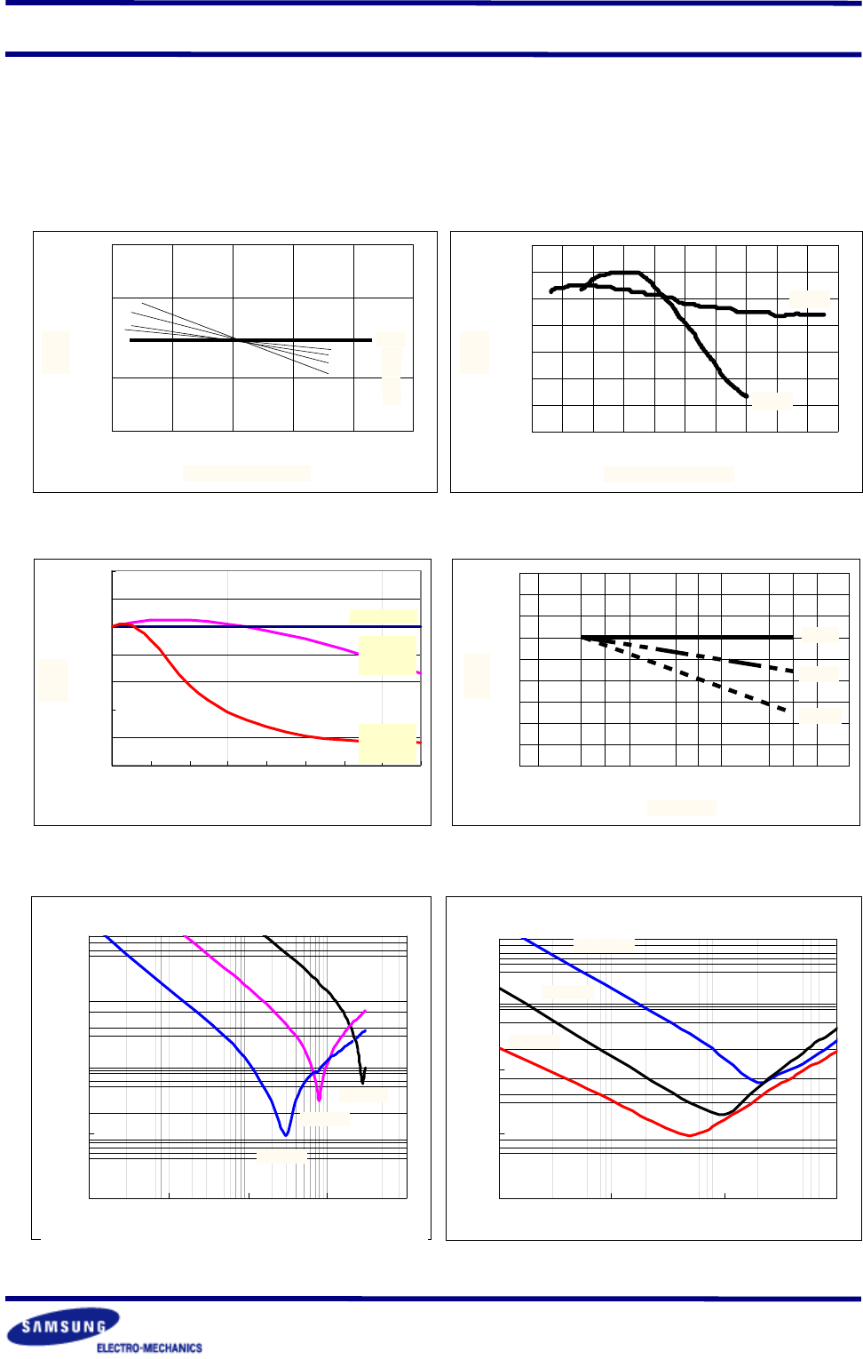
Multilayer Ceramic Capacitor
- 20 -
■
CHARACTERISTIC GRAPH
0 50 100 1000 10000
0
10
-10
-20
-30
Time(Hr)
Δ
C
%
C0G
X7R
Y5V
▶
CAPACITANCE CHANGE - AGING
-60 1400-20 20 60 100
Temperature(
℃
)
Δ
C
%
0
5
-5
-10
10
C0G
UJ
TH
RH
SH
▶
IMPEDANCE - FREQUENCY CHARACTERISTICS
▶
CAPACITANCE - DC VOLTAGE CHARACTERISTICS
C0G
0.01
0.1
1
10
100
1.E +06 1.E+07 1.E+08 1.E +09 1.E+10
Ohm
1MHz 10MHz 100MHz 1GHz
10GHz
1000pF
100pF
10pF
X7R/Y5V
0.01
0.1
1
10
100
1.E+06 1.E+07 1.E+08 1.E+09
Ohm
0.1
㎌
0.01
㎌
0.001
㎌
1MHz 10MHz 100MHz 1GHz
-100
-80
-60
-40
-20
0
20
40
0 5 10 15 20 25 30 35 40
DC V oltage(V dc)
C0G 50V
Δ
C
%
X7R
50V
Y5V
50V
-60 1200-20 20 40 80
-80
-60
-40
-20
0
20
X7R
Y5V
Temperature(
℃
)
Δ
C
%
▶
CAPACITANCE - TEMPERATURE CHARACTERISTICS
●
ELECTRICAL CHARACTERISTICS
Multilayer Ceramic Capacitor
- 21 -
■
APPLICATION MANUAL
●
Storage of products.
▶
Storage Environment
Tape packing materials are designed to withstand long-term storage, but they will degrade more
rapidly in the presence of high temperature or high humidity, therefor, the products must be
stored in an ambient temperature of less than 40
℃
witharelativehumidityoflessthan70%.
Allowable storage period is within 6 months from the outgoing date of delivery.
▶
Corrosive Gases
Since sulfur and chlorine may degrade the solderability of the end termination, it is important t o
store the capacitors in an environment free of these gases.
▶
Temperature Fluctuations
Since dew condensation may occur by the differences in temperature when the products are
taken out of storage, it is important to maintain a temperature-controlled environment.
●
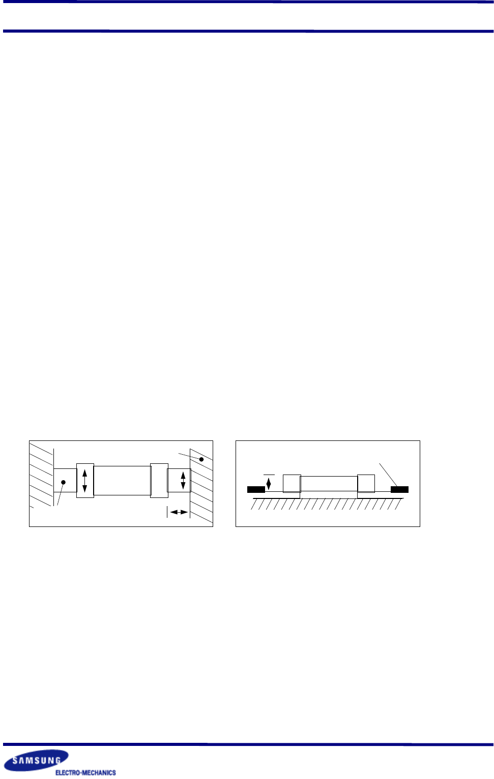
Design of Solder Land Pattern
When designing priented circuit boards, the shape and size of the solder lands must allow f or
the proper amount of solder on the capacitor. The amount of solder at the end terminations
has a direct effect on the probability that the chip will crack. The greater amount of solder, the
amount of stress on the chip, and the more likely that it will break. Use the following illustrations
as guidelines for proper solder land design.
Recommendation of Solder Land Shape and Size
W b
a
Solder
Land
Solder Resist
2/3W < b < W
T
Solder Resist
2/3T < a < T
●
Adhesives
MlCCs generally require the use of an adhesive to position the chips to the circuit board prior
to soldering.
▶
Requirements for Adhesives
They must have enough adhesion so that the chips will not fall off or move during the handling
of the circuit board.
They must maintain their adhesive strength when exposed to soldering temperature.
They should not spread or run when applied to the circuit board.
They should have a long pot life.
They should harden quickly.
They should not c orrode the circuit board or chip material.