HS50 circuit diagram - 第138页
4 Printed Circui t Boards 139 I 0033269 1-010 101ND 3 Video multiple xer , KSP- VMP-HS -50 R55 R75 R74 R73 R72 R71 R70 R30 R29 R28 R27 R2 6 R25 R8 R12 R11 N1 C4 C3 C1 R66 R52 R9 D3 C27 X6 V4 V 3 V2 V1 R82 R68 R67 R61 R46…
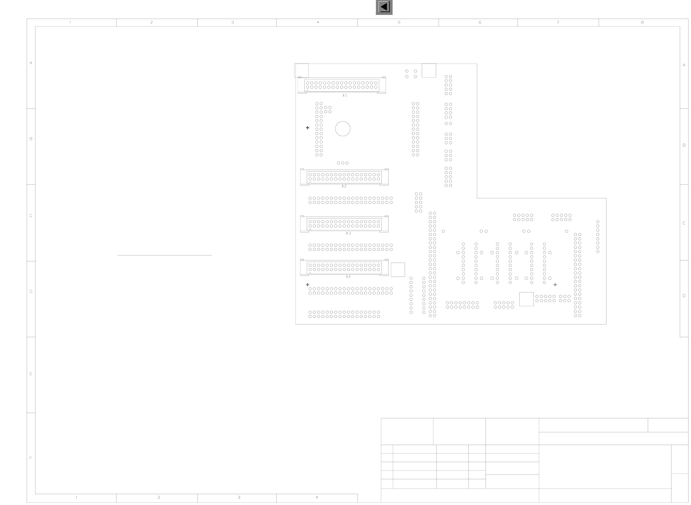
4 Printed Circuit Boards 137
I
00331451-020201ND3 826 board, C50 head board (Sh. 2 of 2)
02
01 26.03.97
20.07.97
KL
KL
ATD TD MCH 2
SIEMENS AG
26.03.97
Klose
00331451-020201ND3
Main board
C50 head board
826 board
G32918-J0008-B001-*-0017
Mounting diagram, solder side
4-layer printed circuit board
2
2
Stat. Modified Date Name
Date
Name
Scale 1:1
Sheet
Sh.
X1
X3
X4
X2
AssemblyPlug
To X1 of gantry distributor 00335413
To X4 of gantry distributor 00335413
To X3 of gantry distributor 00335413
To X2 of gantry distributor 00335413
Please note: X5 will not be fitted
04 09.05.00 KL
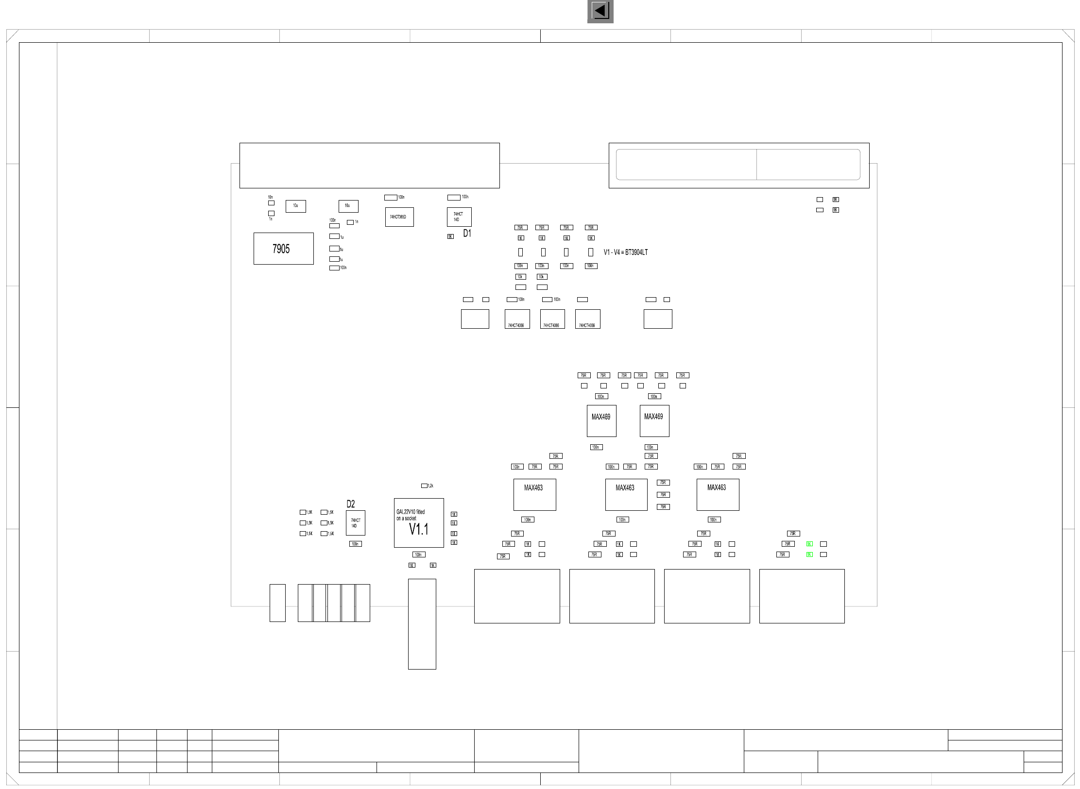
4 Printed Circuit Boards 139
I
00332691-010101ND3 Video multiplexer, KSP-VMP-HS-50
R55
R75
R74
R73
R72
R71
R70
R30
R29R28
R27R26
R25
R8
R12
R11
N1
C4
C3
C1
R66
R52
R9
D3
C27
X6
V4
V
3
V2 V1
R82
R68 R67
R61
R46
R42
R40 R38
R36
R81 R80
R20 R19
R83
R7
R69
R23
R22
R21
R2
R18R17R16
R15
R13
R10
D9
D6
D13
D12
D5 D4
C8
C7
C6
C5
C2
C32
C31
C30
C13 C12C11
C9
C29C28 C26
C23
C20
C17
X5
R65
R64
R63
R60 R56
R50
R49R48
R47
R45
R44R43
R41R39
R37
R35
R33
R84
R77
R76
R6R5R4
R34
R3 R1
D8 D7
D14
D11D10
C34
C25
C24
C22 C21
C19C18
C16 C15
=
SIEMENS AG
+
B
432
567
KSP-VMP-HS50
1
8
F
D
2
64-pole multipoint connector
64-pole multipoint connector
H1 - H6 : green LEDs
R59 R57R53
H1
R54
X4
S1
R62
R51
R79
R78
R32
R31
R24R14
H6H5H4H3H2
C14
C10
X3 X2 X1
R58
Disconnecting switch
MADE IN GERMANY
SIEMENS
TZ
KSP-VMP-S50 LB-XXXXXXXX
00332691-01
KS:026AR1314-0BB00-0AA0
AUT 5
X1 - X 4 : 15-pole connector, Sub D
Components without designation will not be fitted!
Stand.Status Modified NameDate Orig. Repl. f. Replaced by
Check.
Date
Author
Sheet
Sh.
34
B
A
8
1
C
E
5
C
D
E
F
76
A
Geb.
Geb.
1.
1.
1.
18.09.98
18.09.98
18.09.98
18.09.1998
Geb.
Video multiplexer
00332691-010101ND3
PL EA1 E2
1
1
Geb.
besondere fuer den Fall der Patenterteilung oder GM-Eintragung.
nicht ausdruecklich zugestanden. Alle Rechte vorbehalten, ins-
wertung und Mitteilung ihres Inhalts nicht gestattet, soweit
Weitergabe sowie Vervielfaeltigung dieser Unterlage, Ver-
Bauteilangaben nur zur Information Confiado como secrete industrial. Nos reservamos todos los derechos.
Proprietary data , company confidential . All rights reserved.
Confie a titre de secret d’entreprise. Tous droits reserves.
Comunicado como segredo empresarial. Reservados todos os direitos.
Function status
Product status
Doc. status
SMD Placement System SIPLACE HS50
4 Printed Circuit Boards 140
I
00333635-010201ND4 836 board, backplane AC 12.5 (Sh. 1 of 2)
00333635-010201ND4 836 board, backplane AC 12,5 (Sh. 2 of 2)
G32918-J0018-B001-*-0017
2-layer printed circuit board
Mounting diagram, component side
836 board
AC 12.5 backplane
00333635-010201ND4
2
1
SIEMENS AG
10.12.98
Goller
22.07.97
25.11.97
30.06.97
KL
KL
KL01
02
03
Stat. Modified Date Name
Date
Name
Scale 1:1
Sheet
Sh.
03
10.12.98 KL
Enable
5
10
4
3
1, 8, 9, 13, 14
2, 6
X3
n.u.
Inom - W12
3
2
1
X4
GND
Tacho -
Tacho +
2
1
X5
3 Crash signal
Tacho +
Tacho -
4 + 15 V
5n.u.
X6
1, 3
2, 4 - 15 V
+ 15 V
2, 4
1, 3
X7
GND
Link voltage
2
3
4
1
X8
MOTOR_W
MOTOR_V
MOTOR_U
GND
Socket
= pinch off key pin
G
3
2
918-J0018-B001-*-0017
2
-
l
a
y
e
r
printed circuit board
M
o
u
n
t
i
ng diagram, solder side
8
3
6
board
A
C
1
2.5 backplane
0
0
3
3
3635-010201ND4
2
2
S
I
E
M
E
N
S
A
G
1
0
.
1
2
.
9
8
G
o
l
l
e
r
22.07.97
25.11.97
30.06.97
KL
KL
KL01
02
03
B
=
i
n
s
p
e
c
t
i
o
n
l
a
b
e
l
A
=
i
d
e
n
t
i
f
i
c
a
t
i
o
n
l
a
b
el
Stat. Modified Date Name
D
a
t
e
N
a
m
e
S
c
a
l
e
1
:1
Sheet
Sh.
03
10.12.98 KL
X8
X
6
X7
1
2
1
2
Crash signal
Ready
I²t
Inom - U