141-400-57-probestationaccessoriescatalog.pdf_-_141-400-probestationaccessoriescatalog_1.pdf.pdf - 第26页
PN 141-400 www.formfactor.com Cryogenic and Vacuum • 10 Revision 57, February, 2023 Probe Station A ccessories PM V 2 00 W af er Ca rr ie r s 142 36 1 — W af er Car ri er , 200 mm, HF - R eady , PM V20 0 Feat ur es • For…

PN 141-400 www.formfactor.com Cryogenic and Vacuum • 9
Revision 57, February, 2023 Probe Station Accessories
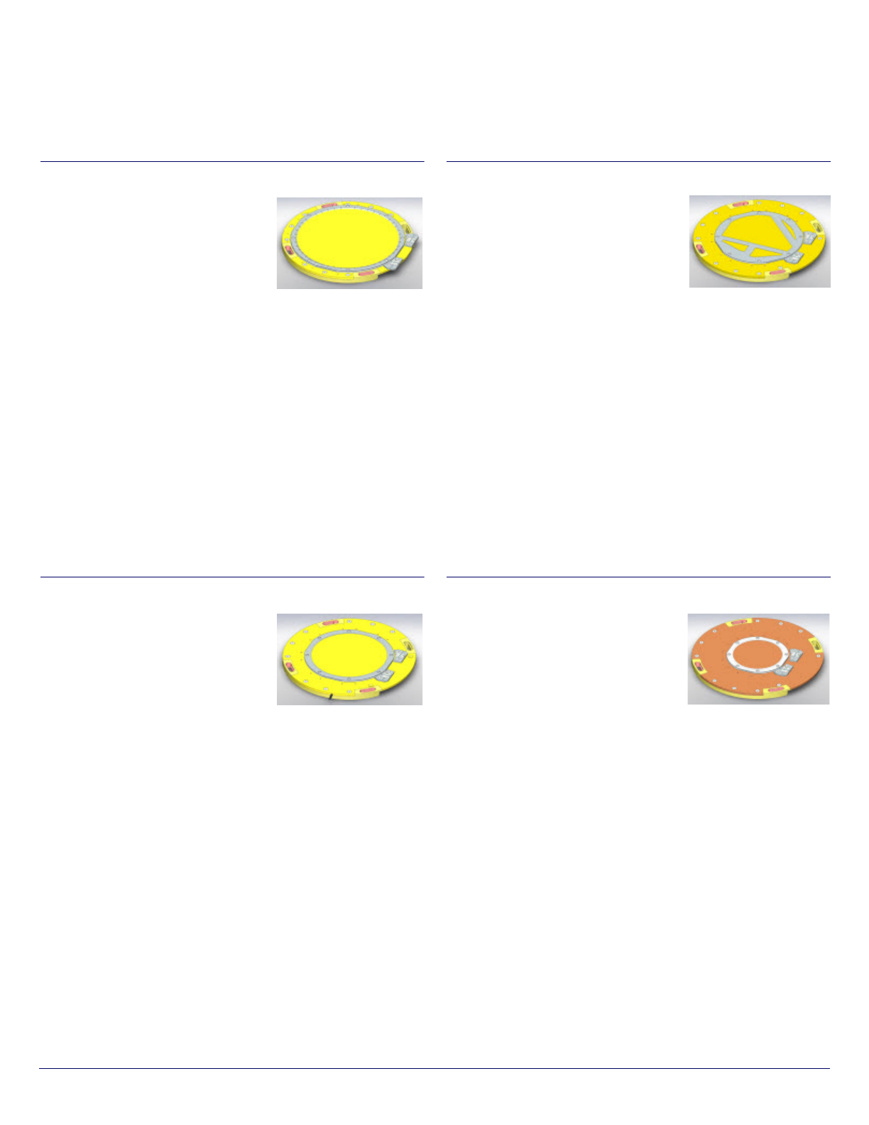
136397 — Universal Carrier, PMC200
Features
• For mounting, fixing and handling of
substrates of different shapes or
wafers up to 75 mm (3 in) wi th
FormFactor cryogenic probe stations
• Mounting outside vacuum chamber
recommended
• Patented mechanical substrate/wafer clamping: mechanical
clamping from top by a universal cla mping mask (top-side
substrate/wafer contact only at the edge)
• Contact plate made of nickel/gold coated OFHC copper for best
heat contact between wafer and chuck
Specifications
• Maximum substrate dimensions:
– 76.2 mm (3 in) (full wafer)
– 150 mm (6 in) (quartered wafer)
– 76.2 x 76.2 mm (3 x 3 in) or 50 x 110 mm (2 x 4.3 in)
Compatibility
• PMC200
PN 141-400 www.formfactor.com Cryogenic and Vacuum • 10
Revision 57, February, 2023 Probe Station Accessories
PMV200 Wafer Carriers
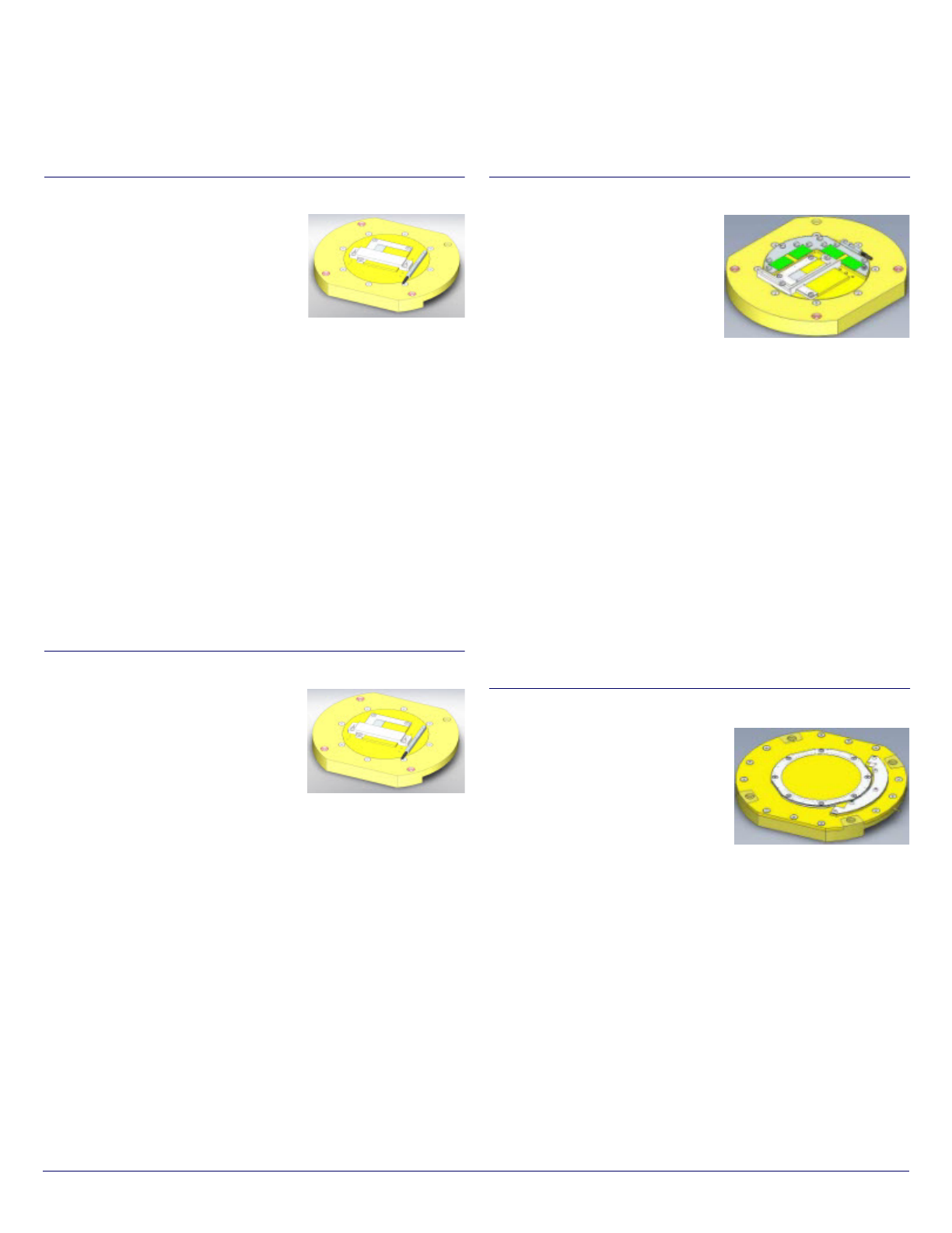
142361 — Wafer Carrier, 200 mm, HF-Ready, PMV200
Features
• For fixing and handling of wafer, wafer
fragments and single chips
• Mounting outside vacuum chamber
recommended
• Patented mechanical clamping
system: mechanical clamping from top by leaf springs (top-side
substrate/wafer contact only at the edge)
• Contact plate made of nickel/gold coated OFHC copper for good
thermal contact between wafer and chuck
• Includes holder for 2 RF calibration substrates
Specifications
• Maximum substrate dimensions:
– 76.2 mm (3 in) (full wafer)
– 150 mm (6 in) (quartered wafer)
– 76.2 x 76.2 mm (3 x 3 in) or 50 x 110 mm (2 x 4.3 in)
• Temperature range: -60° to +200°C (-76° to +392°F)
Compatibility
• PMV200
142365 — Wafer Carrier, 150 mm, HF-Ready, PMV200
Features
• For mounting, fixing and handling of
SEMI s tand ard 150 mm wafers
• Mounting outside vacuum chamber
recommended
• Patented mechanical clamping
system: mechanical clamping from top by a ring shaped leaf spring
(top-side wafer contact only at the edge)
• Contact plate made of nickel/gold coated OFHC copper for good
thermal contact between wafer and chuck
• Includes holder for 2 HF calibration substrates
Specifications
• Temperature range: -60° to +200°C (-76° to +392°F)
Compatibility
• PMV200
144072 — Universal Carrier, PMV200
Features
• For fixing and handling of wafer, wafer
fragments, and single chips
• Mounting outside vacuum chamber
recommended
• Patented mechanical clamping system:
mechanical clamping from top by leaf s prings (top-side substrate/
wafer contact only at the edge)
• Contact plate made of nickel/gold coated OFHC copper for go od
thermal contact between wafer and chuck
• Includes holder for 2 RF calibration substrates
Specifications
• Maximum substrate dimensions:
– 76.2 mm (3 in) (full wafer)
– 150 mm (6 in) ( quartered wafer)
– 76.2 x 76.2 mm (3 x 3 in) or 50 x 110 mm (2 x 4.3 in)
• Temperature range: -60° to +200°C (-76° to +392°F)
Compatibility
• PMV200
144078 — Wafer Carrier, 100 mm, HF-Ready, PMV200
Features
• For mounting, fixing and handling of
SEMI s tandard 100 mm wafers
• Mounting outside vacuum chamber
recommended
• Patented mechanical clamping system:
mechanical clamping from top by a ring shaped leaf spring (top-
side wafer contact only at the edge)
• Contact plate made of nickel/gold coated OFHC copper for go od
thermal contact between wafer and chuck
• Includes holder for 2 HF calibration substrates
Specifications
• Temperature range: -60° to +200°C (-76° to +392°F)
Compatibility
• PMV200
PN 141-400 www.formfactor.com Cryogenic and Vacuum • 11
Revision 57, February, 2023 Probe Station Accessories
PLV50 Wafer Carriers
140971 — Universal Carrier, PLV50
Features
• For fixing and handling of wafer, wafer
fragments, and single chips
• Mounting outside vacuum chamber
recommended
• Patented mechanical clamping
system: mechanical clamping from top by leaf springs (top-side
substrate/wafer contact only at the edge)
• Clamping on three substrate sides with simple adjustment to the
device size by slidable third side piece
• Contact plate made of gold-coated copper for good thermal contact
between wafer and chuck
Specifications
• Maximum substrate dimensions:
– 50.8 mm (2 in) (full wafer)
– 100 mm (4 in) (quartered wafer)
– 50.8 x 50.8 mm (2 x 2 in)
• Temperature range: -60° to +200°C (-76° to +392°F)
Compatibility
• PLV50
155-905 — Universal Carrier, PLV50, 300°
Features
• For fixing and handling of wafer, wafer
fragments, and single chips
• Mounting outside vacuum chamber
recommended
• Patented mechanical clamping
system: mechanical clamping from top by leaf springs (top-side
substrate/wafer contact only at the edge)
• Clamping on three substrate sides with simple adjustment to the
device size by slidable third side piece
• Contact plate made of gold-coated copper for good thermal contact
between wafer and chuck
Specifications
• Maximum substrate dimensions:
– 50.8 mm (2 in) (full wafer)
– 100 mm (4 in) (quartered wafer)
– 50.8 x 50.8 mm (2 x 2 in)
• Temperature range: -60° to +200°C (-76° to +392°F)
Compatibility
• PLV50
141246 — Universal Carrier, HF-Ready, PLV50
Features
• For fixing and handling of wafer,
wafer fragments, single c hips, and
up to four (4) HF calibration
substrates
• Mounting outside vacuum
chamber recommended
• Patented mechanical clamping system: mechanical clamping from
top by leaf springs (top-side substrate/wafer contact o nly at the
edge)
• Clamping on three substrate sides with simple adjustment to the
device size b y slidable third side piece
• Contact plate made of gold-coated copper for g ood thermal contact
between wafer and chuck
Specifications
• Maximum substrate dimensions:
– 50.8 mm (2 in) (full wafer)
– 100 mm (4 in) ( quartered wafer)
– 50.8 x 50.8 mm (2 x 2 in)
• Temperature range: -60° to +200°C (-76° to +392°F)
Compatibility
• PLV50
147917 — Wafer Carrier, 100 mm, PLV50
Features
• For mou nting, fixing and han dling of
SEMI s tandard 100 mm wafers with
Vacuum probe stations
• For use with temperature controlled
chuck systems up to 200°C
• Mounting outside vacuum chamber
recommended
• Patented mechanical wafer clamping: mechanical clamping from
top by a ring s haped leaf spring (top-side wafer contact only at the
edge)
• Contact plate made of nickel/gold coated OFHC copper for be st
heat contact between wafer and chuck
Specifications
• Temperature range: -60° to +200°C (-76° to +392°F)
Compatibility
• PLV50