IPC-SM-782A-表面贴装焊盘图形设计标准.pdf.pdf - 第110页
6.0 TOLERANCE AND SOLDER JOINT ANALYSIS Figure 4 provides an analysis of tolerance assumptions and resultant solder joints based on the land pattern dimensions shown in Figure 3. Tolerances for the component dimensions, …
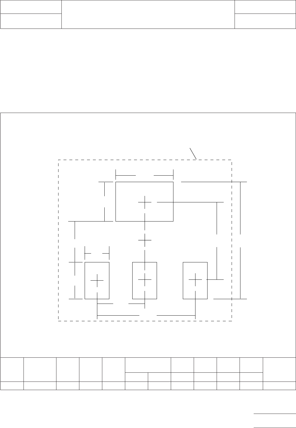
5.0 LAND PATTERN DIMENSIONS
Figure 3 provides the land pattern dimensions for SOT 223
components. These numbers represent industry consensus
on the best dimensions based on empirical knowledge of fab-
ricated land patterns.
In the table, the dimensions shown are at maximum material
condition (MMC). The least material condition (LMC) should
not exceed the fabrication (F) allowance shown on page 4.
The LMC and the MMC provide the limits for each dimension.
The dotted line in Figure 3 shows the grid placement court-
yard which is the area required to place land patterns and
their respective components in adjacent proximity without
interference or shorting. Numbers in the table represent the
number of grid elements (each element is 0.5 by 0.5 mm) in
accordance with the international grid detailed in IEC publica-
tion 97.
RLP
No.
Component
Identifier Z (mm) G (mm)
X1
(mm)
X2 (mm) Y (mm) C (mm)
E1
(mm)
E2
(mm)
Placement
Grid
(No. of Grid
Elements)
min max ref ref basic basic
230 SOT 223 8.40 4.00 1.20 3.40 3.60 2.20 6.20 2.30 4.60 18x14
Figure 3 SOT 223 land pattern dimensions
Z
X2
Y
X1
G
C
E1
▼
▼
▼
▼
▼
▼
▼
▼
▼
▼
▼
▼
▼
▼
Y
▼
▼
▼
Grid placement courtyard
▼
▼
E2
IPC-782-8-10-3
IPC-SM-782
Subject
SOT 223
Date
8/93
Section
8.10
Revision
Page3of4
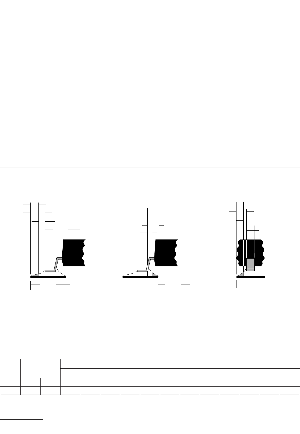
6.0 TOLERANCE AND SOLDER JOINT ANALYSIS
Figure 4 provides an analysis of tolerance assumptions and
resultant solder joints based on the land pattern dimensions
shown in Figure 3. Tolerances for the component dimensions,
the land pattern dimensions (fabrication tolerances on the
interconnecting substrate), and the component placement
equipment accuracy are all taken into consideration.
Figure 4 provides the solder joint minimums for toe, heel, and
side fillets, as discussed in Section 3.3. The tolerances are
addressed in a statistical mode, and assume even distribution
of the tolerances for component, fabrication, and placement
accuracy.
Individual tolerances for fabrication (‘‘F’’) and component
placement equipment accuracy (‘‘P’’) are assumed to be as
given in the table. These numbers may be modified based on
user equipment capability or fabrication criteria. Component
tolerance ranges (C
L
,C
S
, and C
W
) are derived by subtracting
minimum from maximum dimensions given in Figure 2. The
user may also modify these numbers, based on experience
with their suppliers. Modification of tolerances may result in
alternate land patterns (patterns with dimensions other than
the IPC registered land pattern dimensions).
The dimensions for minimum solder fillets at the toe, heel, or
side (J
T
,J
H
,J
S
) have been determined based on industry
empirical knowledge and reliability testing. Solder joint
strength is greatly determined by solder volume. An observ-
able solder fillet is necessary for evidence of proper wetting.
Thus, the values in the table usually provide for a positive sol-
der fillet. Nevertheless, the user may increase or decrease the
minimum value based on process capability.
RLP
No.
Tolerance
Assumptions
(mm)
Solder Joint
Toe (mm) Heel (mm) Side 1 (mm) Side 2 (mm)
FPC
L
J
T
min J
T
max C
S
H
H
min J
H
max C
W1
J
S1
min J
S1
max C
W2
J
S2
min J
S2
max
230 0.2 0.2 0.60 0.52 0.85 0.825 0.03 0.46 0.20 0.10 0.30 0.20 0.13 0.35
Figure 4 Tolerance and solder joint analysis
Zmax
Lmin
▼
▼
▼
▼
1
/2 T
T
J
T
min
Zmax = Lmin + 2J
T
min + T
T
Where:
J
T
min = Minimum toe fillet
T
T
= Combined tolerances
at toe fillet
Smax
J
H
min
Gmin = Smax - 2J
H
min - T
H
Where:
J
H
min = Minimum heel fillet
T
H
= Combined tolerances
at heel fillet
1
/2 T
H
Xmax
Xmax = Wmin + 2J
S
min + T
S
Where:
J
S
min = Minimum side fillet
T
S
= Combined tolerances
at side fillet
▼
▼
Toe Fillet
▼
▼
▼
Heel Fillet Side Fillet
▼
▼
▼
▼
▼
J
T
max
J
H
max
J
S
min
▼
▼
▼
▼
▼
▼
▼
▼
▼
▼
▼
▼
▼
▼
▼
Gmin
▼
1
/2 T
S
J
S
max
▼
▼
▼
Wmin
▼
IPC-782-8-10-4
IPC-SM-782
Subject
SOT 223
Date
8/93
Section
8.10
Revision
Page4of4
1.0 SCOPE
This subsection provides the component and land pattern
dimensions for TO 252 (small outline transistor) components.
Basic construction of the TO 252 device is also covered. At
the end of this subsection is a listing of the tolerances and
target solder joint dimensions used to arrive at the land pat-
tern dimensions.
2.0 APPLICABLE DOCUMENTS
See Section 8.0 for documents applicable to the subsections.
2.1 Electronic Industries Association (EIA) JEDEC Pub-
lication 95 Registered and Standard Outlines for Solid State
and Related Products, TO-252, Issue ‘‘B’’ dated 9/88
Application for copies should be addressed to:
Global Engineering Documents
1990 M Street N.W.
Washington, DC
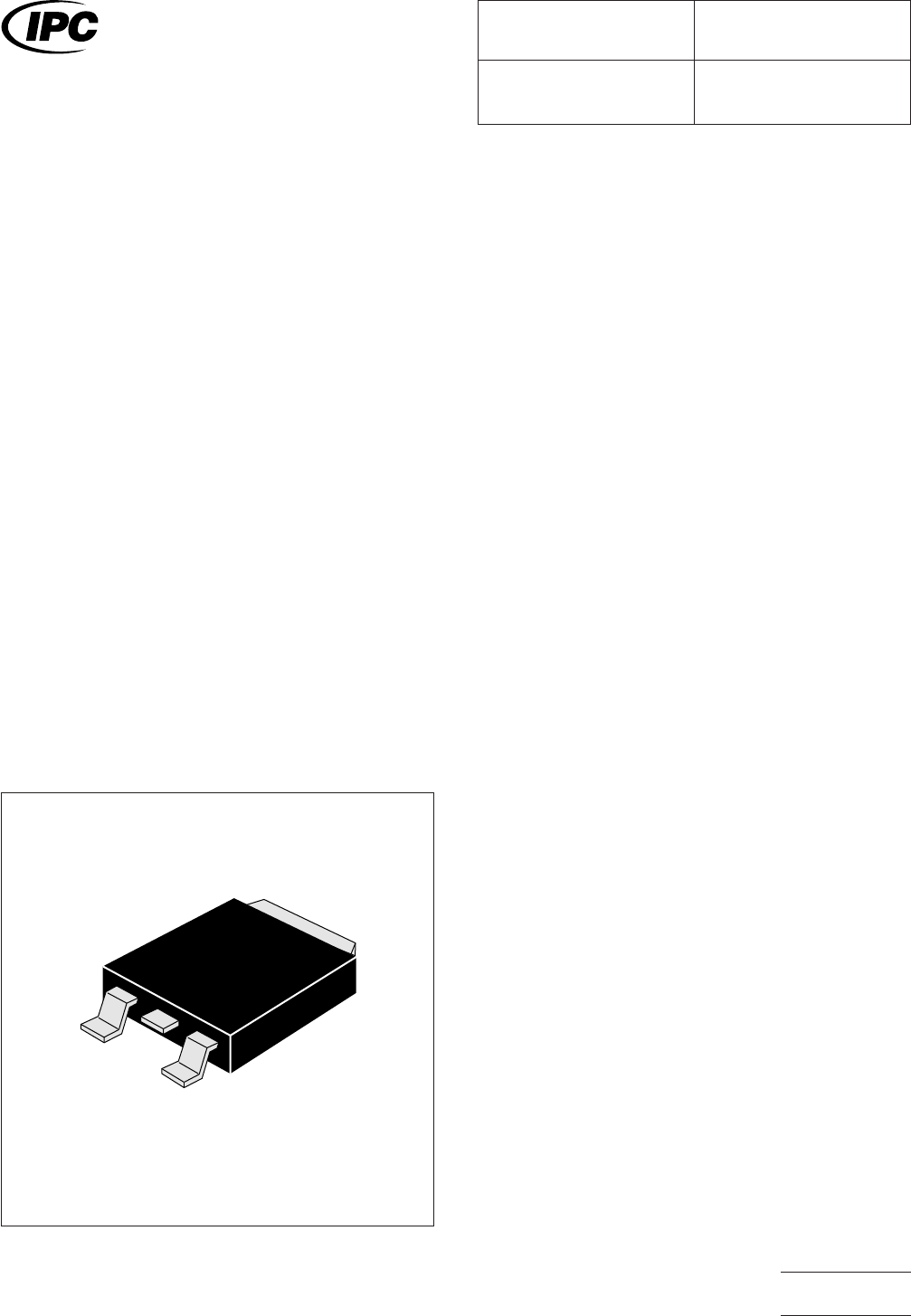
3.0 COMPONENT DESCRIPTIONS
These parts are for dual diodes and Darlington transistors.
3.1 Basic Construction See Figure 1.
3.1.1 Termination Materials Leads should be solder-
coated with a tin/lead alloy. The solder should contain
between 58 to 68% tin. Solder may be applied to the leads by
hot dipping or by plating from solution. Plated solder termina-
tions should be subjected to post-plating reflow operation to
fuse the solder. The tin/lead finish should be at least 0.0075
mm [0.0003 in] thick.
Solder finish applied over precious metal electrodes should
have a diffusion barrier layer between the electrode metalliza-
tion and the solder finish. The barrier layer should be nickel or
an equivalent diffusion barrier, and should be at least 0.00125
mm [0.00005 in] thick.
3.1.2 Marking Parts are available with or without marked
values.
3.1.3 Carrier Package Format Carrier package format
shall be according to the following: body type TO-252, 12 mm
tape/8 mm pitch.
3.1.4 Resistance to Soldering Parts should be capable of
withstanding five cycles through a relow system operating at
215°C. Each cycle shall consist of 60 seconds exposure at
215°C. Parts must also be capable of withstanding a mini-
mum of 10 seconds immersion in molten solder at 260°C.
IPC-782-8-11-1
Figure 1 TO 252 construction
IPC-SM-782
Surface Mount Design
and Land Pattern Standard
Date
5/96
Section
8.11
Revision
A
Subject
TO 252/TO 268
Page1of4