IPC-SM-782A-表面贴装焊盘图形设计标准.pdf.pdf - 第137页
1.0 INTRODUCTION This section covers land patterns for components with J leads on two sides. Each subsection con- tains information in accordance with the following format: 1.0 Scope 2.0 Applicable Documents 3.0 General …
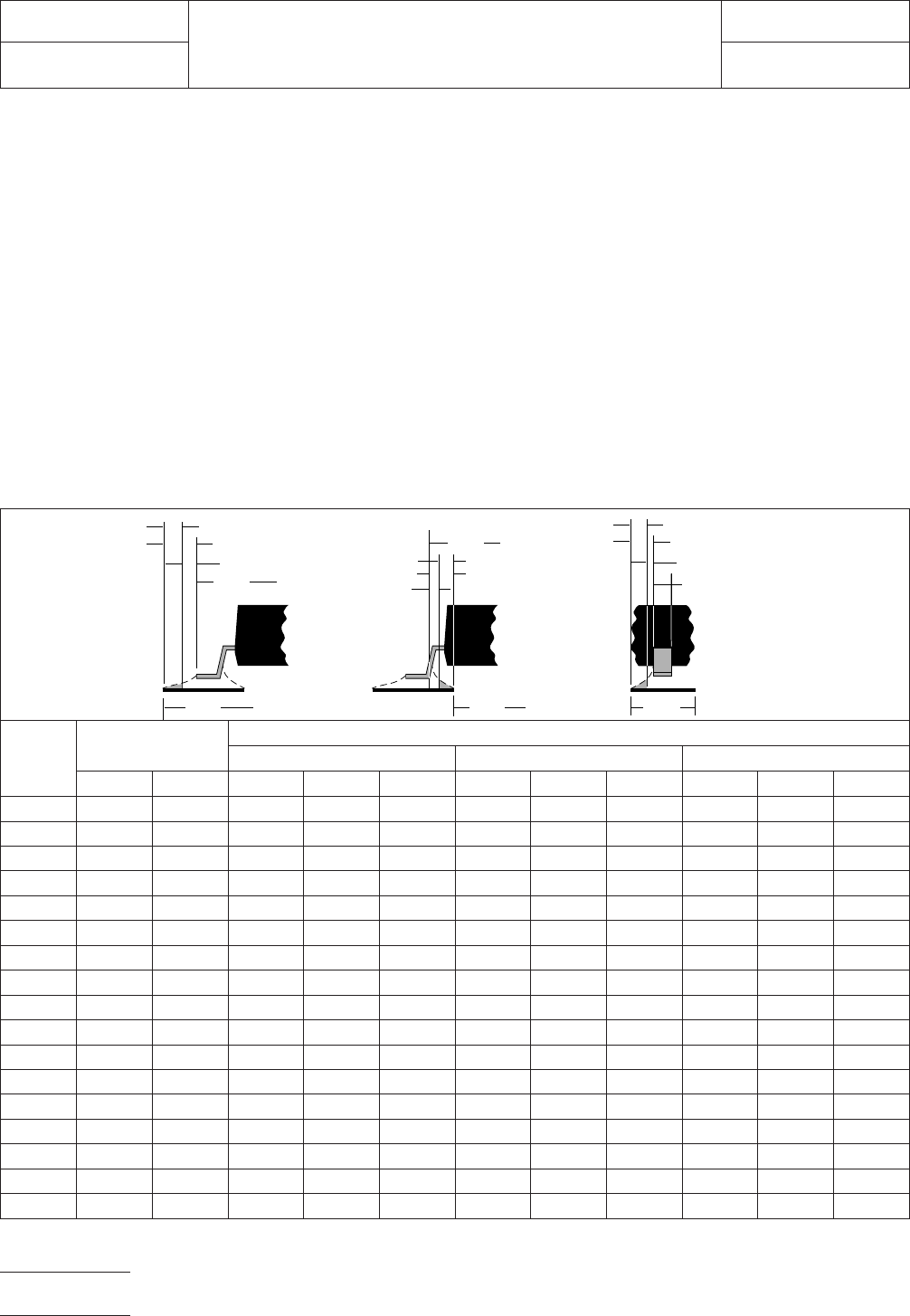
6.0 TOLERANCE AND SOLDER JOINT ANALYSIS
Figure 4 provides an analysis of tolerance assumptions and
resultant solder joints based on the land pattern dimensions
shown in Figure 3. Tolerances for the component dimensions,
the land pattern dimensions (fabrication tolerances on the
interconnecting substrate), and the component placement
equipment accuracy are all taken into consideration.
Figure 4 provides the solder joint minimums for toe, heel, and
side fillets, as discussed in Section 3.3. The tolerances are
addressed in a statistical mode, and assume even distribution
of the tolerances for component, fabrication, and placement
accuracy.
Individual tolerances for fabrication (‘‘F’’) and component
placement equipment accuracy (‘‘P’’) are assumed to be as
given in the table. These numbers may be modified based on
user equipment capability or fabrication criteria. Component
tolerance ranges (C
L
,C
S
, and C
W
) are derived by subtracting
minimum from maximum dimensions given in Figure 2. The
user may also modify these numbers, based on experience
with their suppliers. Modification of tolerances may result in
alternate land patterns (patterns with dimensions other than
the IPC registered land pattern dimensions).
The dimensions for minimum solder fillets at the toe, heel, or
side (J
T
,J
H
,J
S
) have been determined based on industry
empirical knowledge and reliability testing. Solder joint
strength is greatly determined by solder volume. An observ-
able solder fillet is necessary for evidence of proper wetting.
Thus, the values in the table usually provide for a positive sol-
der fillet. Nevertheless, the user may increase or decrease the
minimum value based on process capability.
RLP No.
Tolerance
Assumptions (mm)
Solder Joint
Toe (mm) Heel (mm) Side (mm)
FPC
L
J
T
min J
T
max C
S
J
H
min J
H
max C
W
T
S
min T
S
max
420 0.2 0.2 0.60 0.27 0.60 0.60 0.30 0.73 0.10 0.05 0.20
421 0.2 0.2 0.60 0.27 0.60 0.60 0.30 0.73 0.10 0.05 0.20
422 0.2 0.2 0.60 0.27 0.60 0.60 0.31 0.73 0.08 –0.02 0.14
423 0.2 0.2 0.60 0.27 0.60 0.60 0.31 0.73 0.10 –0.02 0.14
424 0.2 0.2 0.60 0.27 0.60 0.60 0.31 0.73 0.10 –0.02 0.14
425 0.2 0.2 0.60 0.27 0.60 0.60 0.31 0.73 0.10 0.05 0.20
426 0.2 0.2 0.60 0.27 0.60 0.60 0.31 0.73 0.10 –0.02 0.14
427 0.2 0.2 0.60 0.27 0.60 0.60 0.31 0.73 0.10 –0.06 0.10
428 0.2 0.2 0.60 0.27 0.60 0.60 0.31 0.73 0.10 –0.02 0.14
429 0.2 0.2 0.60 0.27 0.60 0.60 0.31 0.73 0.10 0.01 0.16
430 0.2 0.2 0.60 0.27 0.60 0.60 0.31 0.73 0.10 –0.02 0.14
431 0.2 0.2 0.60 0.27 0.60 0.60 0.31 0.73 0.10 –0.02 0.14
432 0.2 0.2 0.60 0.27 0.60 0.60 0.31 0.73 0.10 –0.02 0.14
433 0.2 0.2 0.60 0.27 0.60 0.60 0.31 0.73 0.10 –0.02 0.14
434 0.2 0.2 0.60 0.27 0.60 0.60 0.31 0.73 0.10 –0.06 0.10
435 0.2 0.2 0.60 0.27 0.60 0.60 0.31 0.73 0.10 –0.02 0.14
436 0.2 0.2 0.60 0.27 0.60 0.60 0.31 0.73 0.10 –0.02 0.14
Figure 4 Tolerance and solder joint analysis
Zmax
Lmin
▼
▼
▼
▼
1
/2 T
T
J
T
min
Smax
J
H
min
1
/2 T
H
Xmax
▼
▼
Toe Fillet
▼
▼
▼
Heel Fillet
Side Fillet
▼
▼
▼
▼
▼
J
T
max
J
H
max
J
S
min
▼
▼
▼
▼
▼
▼
▼
▼
▼
▼
▼
▼
▼
▼
▼
Gmin
▼
1
/2 T
S
J
S
max
▼
▼
▼
Wmin
▼
IPC-782-9-5-4
IPC-SM-782
Subject
CFP
Date
8/93
Section
9.5
Revision
Page4of4

1.0 INTRODUCTION This section covers land patterns for
components with J leads on two sides. Each subsection con-
tains information in accordance with the following format:
1.0 Scope
2.0 Applicable Documents
3.0 General Component Description (Figure 1)
4.0 Component Dimensions (Figure 2)
5.0 Land Pattern Dimensions (Figure 3)
6.0 Tolerance and Solder Joint Analysis (Figure 4)
The following is the table of contents for this section:
Table of Contents
Section Component
10.1 SOJ
2.0 APPLICABLE DOCUMENTS
The following documents, of the issue in effect on the revision
date of this section, form a part of this specification to the
extent specified herein.
2.1 Electronic Industries Association (EIA)
1
JEDEC Publication 95 Registered and Standard Outlines for
Solid State and Related Products:
MO-077, issue ‘‘C,’’ dated 8/91
MO-065, issue ‘‘A,’’ dated 5/87
MO-063, issue ‘‘A,’’ dated 4/2/87
MO-061, issue ‘‘C,’’ date 8/91
EIA-PDP-100 Registered and Standard Mechanical Outlines
for Electronic Parts
EIA-481-A Taping of Surface Mount Components for Auto-
matic Placement
EIA-481-3 32 mm, 44 mm, and 56 mm Embossed Carrier
Taping of Surface Mount Components for Automated Han-
dling
2.2 Electronic Industries Association of Japan (EIAJ)
EIAJ-ED-7406
General Rules for the Preparation of Outline
Drawings of Integrated Circuits
2.3 International Electrotechnical Commission (IEC)
2
IEC 97 Grid Elements
3.0 General Information
3.1 General Component Description
This section pro-
vides the component and land pattern dimensions for small
outline integrated circuits with ‘‘J’’ leads (SOJ components).
Basic construction of the SOJ device is also covered. At the
end of the subsections are listings of the tolerances and tar-
get solder joint dimensions used to arrive at the land pattern
dimensions.
3.2 Packaging Components may be provided in tube or
tape packaging. Tape is preferred for best handling and high
volume applications. Bulk packaging is not acceptable
because of lead coplanarity requirements required for place-
ment and soldering. EIA-481 provides details on tape require-
ments.
1. Application for copies should be addressed to Global Engi-
neering Documents, 1990 M St. N.W., Washington, DC
20036.
2. Application for copies should be addressed to IEC, 3 rue
de Varembe, PO Box 131 - 1211 Geneva 20, Switzerland
IPC-SM-782
Surface Mount Design
and Land Pattern Standard
Date
8/93
Section
10.0
Revision Subject
Components with J Leads
on Two Sides
Page1of2

Page Intentionally Left Blank
IPC-SM-782
Subject
Components with J Leads on Two Sides
Date
8/93
Section
10.0
Revision
Page2of2