IPC-SM-782A-表面贴装焊盘图形设计标准.pdf.pdf - 第180页
6.0 TOLERANCE AND SOLDER JOINT ANALYSIS Figure 4 provides an analysis of tolerance assumptions and resultant solder joints based on the land pattern dimensions shown in Figure 3. Tolerances for the component dimensions, …
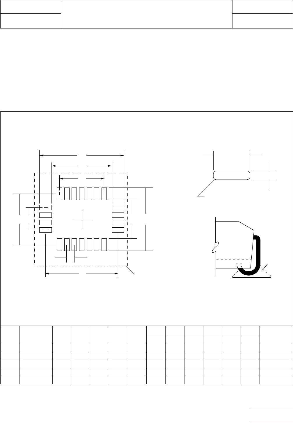
5.0 LAND PATTERN DIMENSIONS
Figure 3 provides the land pattern dimensions for PLCC (Rect-
angular) components. These numbers represent industry con-
sensus on the best dimensions based on empirical knowledge
of fabricated land patterns.
In the table, the dimensions shown are at maximum material
condition (MMC). The least material condition (LMC) should
not exceed the fabrication (F) allowance shown on page 4.
The LMC and the MMC provide the limits for each dimension.
The dotted line in Figure 3 shows the grid placement court-
yard which is the area required to place land patterns and
their respective components in adjacent proximity without
interference or shorting. Numbers in the table represent the
number of grid elements (each element is 0.5 by 0.5 mm) in
accordance with the international grid detailed in IEC publica-
tion 97.
RLP No.
Component
Identifier Z1 (mm)
G1
(mm) Z2 (mm)
G2
(mm) X (mm)
Y (mm) C1 (mm) C2 (mm) D1 (mm) D2 (mm) E (mm)
Placement Grid
(No. of Grid
Elementsref ref ref ref ref ref
810A PLCC/R-18 9.40 5.00 12.80 8.40 0.60 2.00 7.20 10.60 3.81 5.08 1.27 22x28
811A PLCC/R-18-L 9.40 5.00 14.40 10.00 0.60 2.00 7.20 12.20 3.81 5.08 1.27 22x32
812A PLCC/R-22 9.40 5.00 14.40 10.00 0.60 2.00 7.20 12.20 3.81 7.62 1.27 22x32
813A PLCC/R-28 11.00 6.60 16.00 11.60 0.60 2.00 8.80 13.80 5.08 10.16 1.27 24x34
814A PLCC/R-32 13.60 9.20 16.00 11.60 0.60 2.00 11.40 13.80 7.62 10.16 1.27 30x34
Figure 3 PLCC (Rectangular) land pattern dimensions
Z2
G2
C2
Full radius
optional
▼
▼
▼
▼
▼
▼
Heel
D2
D1C1
▼
▼
▼
▼
G1 Z1
▼
▼
▼
▼
▼
▼
E
Y
X
Grid placement
courtyard
▼
IPC-782-12-2-3
IPC-SM-782
Subject
PLCC (Rectangular)
Date
5/96
Section
12.2
Revision
A
Page3of4
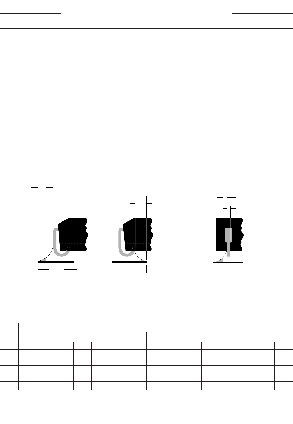
6.0 TOLERANCE AND SOLDER JOINT ANALYSIS
Figure 4 provides an analysis of tolerance assumptions and
resultant solder joints based on the land pattern dimensions
shown in Figure 3. Tolerances for the component dimensions,
the land pattern dimensions (fabrication tolerances on the
interconnecting substrate), and the component placement
equipment accuracy are all taken into consideration.
Figure 4 provides the solder joint minimums for toe, heel, and
side fillets, as discussed in Section 3.3. The tolerances are
addressed in a statistical mode, and assume even distribution
of the tolerances for component, fabrication, and placement
accuracy.
Individual tolerances for fabrication (‘‘F’’) and component
placement equipment accuracy (‘‘P’’) are assumed to be
asgiven in the table. These numbers may be modified based
on user equipment capability or fabrication criteria. Compo-
nent tolerance ranges (C
L
,C
S
, and C
W
) are derived by sub-
tracting minimum from maximum dimensions given in Figure
2. The user may also modify these numbers, based on expe-
rience with their suppliers. Modification of tolerances may
result in alternate land patterns (patterns with dimensions
other than the IPC registered land pattern dimensions).
The dimensions for minimum solder fillets at the toe, heel, or
side (J
T
,J
H
,J
S
) have been determined based on industry
empirical knowledge and reliability testing. Solder joint
strength is greatly determined by solder volume. An observ-
able solder fillet is necessary for evidence of proper wetting.
Thus, the values in the table usually provide for a positive sol-
der fillet. Nevertheless, the user may increase or decrease the
minimum value based on process capability.
RLP
No.
Tolerance
Assumptions
(mm)
Solder Joint
Heel 1 and 2 (mm) Toe 1 and 2 (mm) Side 1 and 2 (mm)
FPC
L
J
H1
min J
H1
max J
H2
min J
H2
max C
S
J
T1
min J
T1
max J
T2
min J
T2
max C
W
J
S
min J
S
max
810A 0.10 0.10 0.25 0.53 0.67 0.45 0.60 0.75 –0.48 –0.10 –0.40 –0.02 0.20 0.01 0.14
811A 0.10 0.10 0.38 0.43 0.64 0.39 0.60 0.80 –0.44 –0.03 –0.40 0.01 0.20 0.01 0.14
812A 0.10 0.10 0.38 0.43 0.64 0.39 0.60 0.80 –0.44 –0.03 –0.40 0.01 0.20 0.01 0.14
813A 0.10 0.10 0.25 0.47 0.61 0.43 0.57 0.75 –0.42 –0.04 –0.38 0.00 0.20 0.01 0.14
814A 0.10 0.10 0.25 0.50 0.64 0.43 0.57 0.75 –0.45 –0.06 –0.38 0.00 0.20 0.01 0.14
Figure 4 Tolerance and solder joint analysis
Zmax = Lmin + 2J
T
min + T
T
Where:
J
T
min = Minimum toe fillet
T
T
= Combined tolerances
at toe fillet
Gmin = Smax - 2J
H
min - T
H
Where:
J
H
min = Minimum heel fillet
T
H
= Combined tolerances
at heel fillet
Xmax
Xmax = Wmin + 2J
S
min + T
S
Where:
J
S
min = Minimum side fillet
T
S
= Combined tolerances
at side fillet
▼
▼
Toe Fillet
1
/2 T
S
Heel Fillet Side Fillet
J
S
max
▼
▼
▼
▼
▼
▼
▼
J
S
min
Lmin
▼
▼
Zmax
▼
▼
1
/2 T
T
J
T
min
Smax
J
H
min
1
/2 T
H
▼
▼
▼
▼
▼
▼
▼
▼
J
T
max
J
H
max
▼
▼
▼
▼
▼
▼
▼
▼
▼
▼
▼
Gmin
▼
Wmin
▼
IPC-782-12-2-4
IPC-SM-782
Subject
PLCC (Rectangular)
Date
5/96
Section
12.2
Revision
A
Page4of4
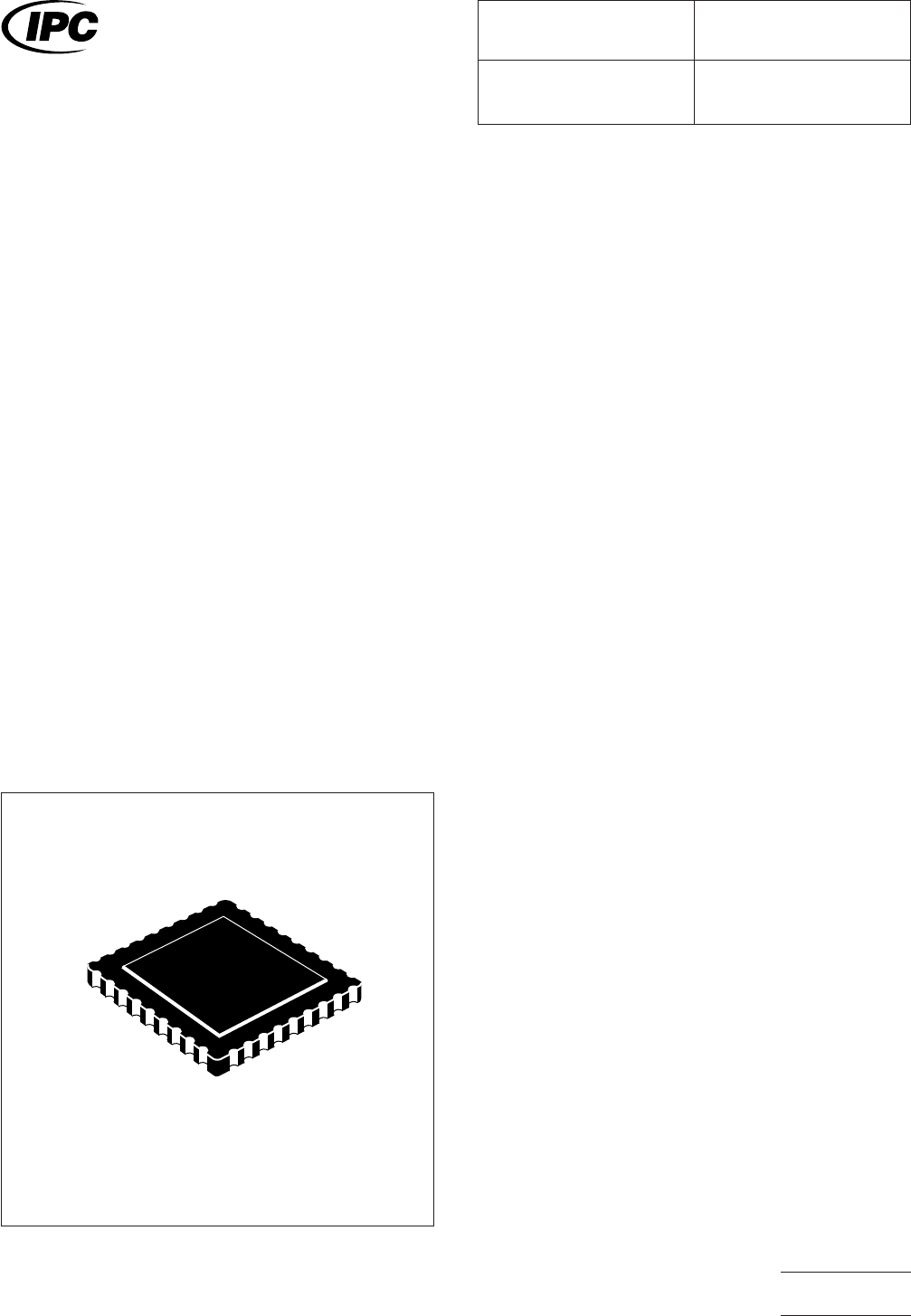
1.0 SCOPE
This subsection provides the component and land pattern
dimensions for leadless ceramic chip carriers (LCC compo-
nents). Basic construction of the LCC device is also covered.
At the end of this subsection is a listing of the tolerances and
target solder joint dimensions used to arrive at the land pat-
tern dimensions.
2.0 APPLICABLE DOCUMENTS
See Section 12.0 and the following for documents applicable
to this subsection.
2.1 Electronic Industries Association (EIA)
JEDEC Publication 95
Registered and Standard Outlines for Solid JEDEC Publication
95 State and Related Products, ‘‘0.050 In. Center, Leadless
Type A,’’ Outline MS002, issue ‘‘A,’’ dated 9/29/80, and
‘‘0.050 In. Center, Leadless Type C,’’ Outline MS004, issue
‘‘B,’’ dated 5/90
3.0 Component Descriptions
3.1 Basic Construction
A leadless chip carrier is a
ceramic package with integral surface-metallized terminations.
Leadless Types A, B, and D chip carriers have a chamfered
index corner that is larger than that of Type C. Another differ-
ence between the A, B, and D types and Type C is the fea-
ture in the other three corners. The types A, B, and D, were
designed for socket applications and printed wiring intercon-
nections. The Type C is primarily intended for direct attach-
ment through reflow soldering. This application difference is
the main reason for their mechanical differences. These pack-
ages mount in different orientations, depending on type,
mounting structure and preferred thermal orientation.
Leadless Type A is intended for lid-down mounting in a
socket, which places the primary heat-dissipating surface
away from the mounting surface for more effective cooling in
air-cooled systems.
Type C is a ceramic package similar to leadless Type B
except for corner configuration. The 50 mil center family,
which includes both leadless and leaded devices, is designed
to mount on a common mounting pattern. They may be
directly attached to the mounting structure, or can be plugged
into sockets. One basic restriction is that there shall be no
terminals in the corners of the package. There are a number
of common sizes.
3.1.1 Termination Materials Leads must be solder-
coated with a tin/lead alloy. The solder should contain
between 58 to 68% tin. Solder may be applied to the leads by
hot dipping or by plating from solution. Plated solder termina-
tions should be subjected to post-plating reflow operation to
fuse the solder. The tin/lead finish should be at least 0.0075
mm [0.0003 in.] thick.
3.1.2 Marking All parts shall be marked with a part num-
ber and ‘‘Pin 1’’ location. Pin 1 location may be molded into
the plastic body.
3.1.3 Carrier Package Format Tube carriers are preferred
for best handling.
3.1.4 Process Considerations LCCs are usually pro-
cessed using standard solder reflow processes. Parts should
be capable of withstanding ten cycles through a standard
reflow system operating at 215°C. Each cycle shall consist of
60 seconds exposure at 215°C.
IPC-782-12-3-1
Figure 1 LCC Construction
IPC-SM-782
Surface Mount Design
and Land Pattern Standard
Date
8/93
Section
12.3
Revision Subject
LCC
Page1of4