IPC-SM-782A-表面贴装焊盘图形设计标准.pdf.pdf - 第194页
5.0 HANDLING AND SHIPPING For information on trays and shipping containers refer to ACH:EIA-481-A, ACH:EIA-481-3, JEDEC CO-028, and JEDEC CO-029. 6.0 LAND PATTERN ANALYSIS The following provides an analysis of tolerance …
smaller for pitches less than 1.0 mm. Refer to the manufac-
turer specification before finalizing land pattern array and
geometry.
4.4.1 Copper Defined Land Pattern The land patterns
described are defined by the etched copper. Solder mask
clearance should be a minimum of 0.075 mm from the etched
copper land. For applications requiring a clearance that is less
than recommended, consult with the printed board supplier.
4.4.2 Solder Mask Defined Land Pattern If solder mask
defined patterns are used, then adjust land pattern diameter
accordingly. See Section 6.0.
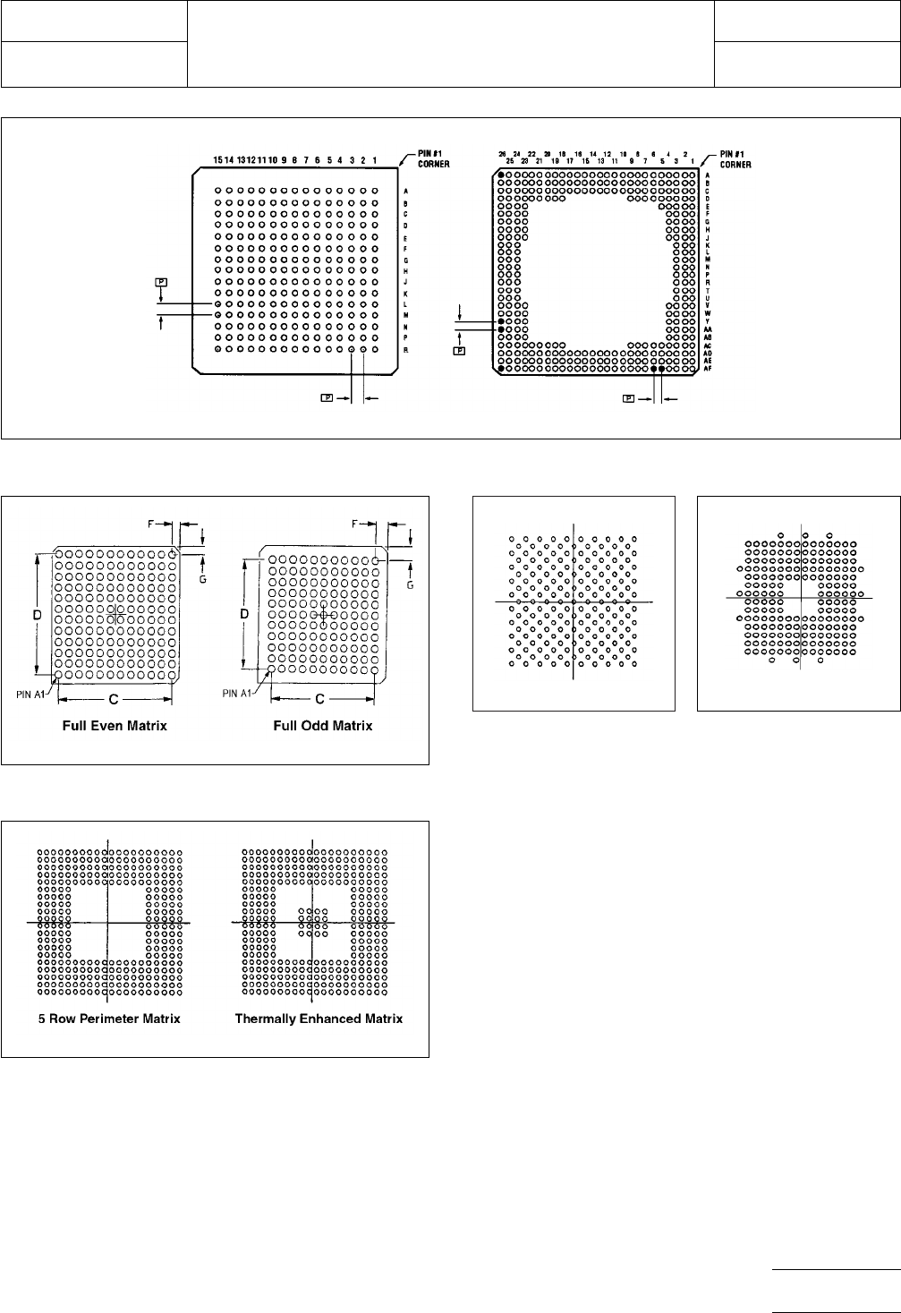
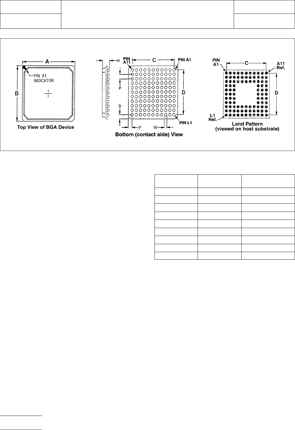
4.5 Defining Contact Assignment Array contact identifi-
cation is assigned by the column and row location. For
example, A1 contact position is always at an outside corner
position with alpha characters arranged in a vertical (row) pat-
tern from top to bottom. Numeric characters are assigned in
a horizontal (column) axis (I, O, Q, S, X and Z are omitted). See
Figure 4-6.
The designer should note that the A1 position is at the upper
left hand corner when the device is viewed from the top. Con-
tact pattern is defined when viewed from the bottom. The land
pattern provided on the host substrate is opposite of the con-
tact pattern (with A1 contact position again at the upper left).
IPC-782144-4
Figure 4-4 Staggered
matrix
IPC-782144-5
Figure 4-5 Selective
depopulation
IPC-782144-1
Figure 4-1 Bottom view of BGA devices
IPC-782144-2
Figure 4-2 One package size, two full matrices
IPC-782144-3
Figure 4-3 Perimeter and thermally enhanced matrices
IPC-SM-782A
Subject
Components with Ball Grid Array Contacts
Date
4/99
Section
14.0
Revision
—
Page3of6
5.0 HANDLING AND SHIPPING
For information on trays and shipping containers refer to
ACH:EIA-481-A, ACH:EIA-481-3, JEDEC CO-028, and
JEDEC CO-029.
6.0 LAND PATTERN ANALYSIS
The following provides an analysis of tolerance assumptions
and result in solder joints based on the land pattern dimen-
sions shown in Figure 4-6. The variations that exist in deter-
mining these land patterns include the diameter of the indi-
vidual ball, the positional accuracy of the ball in relationship to
a true position on the component and the board, and the
manufacturing allowance that can be held for the land on the
substrate that mount the particular ball. The land pattern of
the component (where the ball is attached) and the land pat-
tern of the substrate mounting structure (printed board)
should be as similar as possible. Component manufacturers
have made their determinations that the land pattern of pad
on the component should be less than the ball diameter. They
base their conclusions on the resulting nominal ball diameter
with a slight reduction in the land approximation. Pitch plays a
large role in the determination of what ball diameters can be
used in various combinations. Table 6-1 shows the character-
istics of those balls that are used with pitches of 1.5 mm
through 1.0 mm, as well as future ball sizes whose pitches fall
between 0.80 mm and 0.25 mm.
6.1 Land Approximation In each instance, component
manufacturers and board designers are encouraged to
reduce the land size by some percentage of the nominal ball
diameter. The amount of reduction is based on the original
ball size, which is used to determine the average land. In
determining the relationship between nominal characteristics,
a manufacturing allowance for land size has been determined
to be 0.1 mm between the Maximum Material Condition
(MMC) and Least Material Condition (LMC). Table 6-2 shows
the reduction characteristics, the nominal land size, and the
target land dimensions, as well as future approximations for
ball diameters of 0.40 mm and below.
6.2 Total Variation The total variation of the system con-
siders three major issues: positioning, ball tolerance, and sub-
strate tolerance. All three attributes added together result in a
worst case analysis, however as with other land patterns in
the standard, a statistical average is determined by using the
RMS (root, mean, square) value. Table 6-3 shows the total
variation in the system for each of the four ball sizes identified
in the standard.
It should be noted that the target value for lands on the sub-
strate of the component or the board should be at Maximum
Material Condition. The variation from the Maximum Material
Condition indicates that ball-to-land misalignment is achieved
IPC-782144-6a,b & c
Figure 4-6 Device orientation and contact A1 position
Table 6-1 Ball Diameter Sizes
Nominal Ball
Diameter (mm)
Tolerance
Variation (mm) Pitch (mm)
0.75 0.90 - 0.65 1.5, 1.27
0.60 0.70 - 0.50 1.0
0.50 0.55 - 0.45 1.0, 0.8
0.45 0.50 - 0.40 1.0, 0.8, 0.75
0.40 0.45 - 0.35 0.80, 0.75, 0.65
0.30 0.35 - 0.25 0.8, 0.75, 0.65, 0.50
0.25 0.28 - 0.22 0.40
0.20 0.22 - 0.18 0.30
0.15 0.17 - 0.13 0.25
IPC-SM-782A
Subject
Components with Ball Grid Array Contacts
Date
4/99
Section
14.0
Revision
—
Page4of6
by taking the maximum land size and subtracting the varia-
tion. The resulting dimension would indicate the amount of
attachment area that would result from a system where all
conditions are at a negative instance. For lands that are sol-
der mask-defined, the land size should be increased by the
amount of encroachment of the solder mask. As an example,
if the requirement is that solder mask should be on the land
by 0.05 mm, then the maximum land size should be increased
by 0.1. It should be noted that for solder mask-defined lands,
since the land size increases, the opportunity to route con-
ductors between lands is impacted by reducing the available
area for conductor width and spacing.
6.3 Future Ball Conditions Although not required for the
BGAs shown in the present release of 14.0, future ball sizes
contemplated are shown in Table 6-1. Their land size approxi-
mations are shown in Table 6-2.
6.4 Land Pattern Calculator The land pattern calcula-
tions for BGAs are based on ball size. As a result of ball varia-
tion and component conditions, Table 6-4 shows the land
pattern calculator headings needed to describe the variations
in the system. The RLP number pertains to a single land. It is
applicable to all the registered land pattern numbers for the
various registered packages shown in Section 14. This data is
usually described at the Maximum Material Condition for non-
solder mask-defined lands and is dimension X in the various
sections. The registered single land pattern numbers for the
various ball sizes are shown in Table 6-4.
Table 6-4 Land-to-Ball Calculations for Current and Future BGA Packages (mm)
RLP
Land Size
Location
Allowance
Ball
Variation
PCB
Fabrication
Allowance
Ball Size
%
Reduction
From Nom.
Variation
AllowanceMMC LMC Nominal MMC LMC
050 0.60 0.50 0.10 0.25 0.10 0.75 0.90 0.65 25% 0.25
051 0.50 0.40 0.10 0.20 0.10 0.60 0.70 0.50 25% 0.20
052 0.45 0.35 0.10 0.10 0.10 0.50 0.55 0.45 20% 0.17
053 0.40 0.30 0.10 0.10 0.10 0.45 0.50 0.40 20% 0.17
054 0.35 0.25 0.10 0.10 0.10 0.40 0.45 0.35 20% 0.17
055 0.25 0.20 0.05 0.10 0.05 0.30 0.35 0.25 20% 0.15
056 0.20 0.17 0.05 0.06 0.03 0.25 0.28 0.22 20% 0.08
057 0.15 0.12 0.05 0.04 0.03 0.20 0.22 0.18 20% 0.07
058 0.10 0.08 0.05 0.04 0.02 0.15 0.17 0.13 20% 0.07
Table 6-2 Land Approximation
Nominal Ball
Diameter
(mm) Reduction
Nominal
Land
Diameter
(mm)
Land
Variation
(mm)
0.75 25% 0.55 0.60 - 0.50
0.60 25% 0.45 0.50 - 0.40
0.50 20% 0.40 0.45 - 0.35
0.45 20% 0.35 0.40 - 0.30
0.40 20% 0.30 0.35 - 0.25
0.30 20% 0.25 0.25 - 0.20
0.25 20% 0.20 0.20 - 0.17
0.20 20% 0.15 0.15 - 0.12
0.15 20% 0.10 0.10 - 0.08
Table 6-3 BGA Variation Attributes
Nominal
Ball
Size
(mm)
Positional
Allowance
Ball
Tolerance
(mm)
Substrate
Tolerance
(mm)
Variation
RMS
Value
0.75 0.1 dia. DTP 0.25 0.10 0.25
0.60 0.1 dia. DTP 0.20 0.10 0.24
0.50 0.1 dia. DTP 0.10 0.10 0.17
0.45 0.1 dia. DTP 0.10 0.10 0.17
IPC-SM-782A
Subject
Components with Ball Grid Array Contacts
Date
4/99
Section
14.0
Revision
—
Page5of6