IPC-SM-782A-表面贴装焊盘图形设计标准.pdf.pdf - 第30页
grid based placement rules of the THT boards. This ulti- mately results in components being randomly placed, and vias being even more randomly placed across the board. T wo problems created by random component placement …
the design is memory, general logic, or analog, it is recom-
mended that all component orientations are such that pin
one orientation is the same.
3.6.1.4 Grid-Based Component Placement SMT com-
ponent placement and orientation is generally more difficult
than THT printed boards for two reasons: higher compo-
nent densities, and the ability to put components on both
sides of the board. For THT designs, the component leads
are on 2.54 mm [0.100 in] centers and, assuming 1.3 mm
[0.065 in] lands, the spacing between lands would be 1.2
mm. In high density SMT designs, however, the spacing
between lands is often less, down to 0.63 mm [0.025 in]
and smaller. Grid based component placement (0.100 inch
grid is standard with THT) is complicated by the large
variety of land sizes associated with the SMT component
packages now becoming available. Most SMT designs
being done today have abandoned the 2.54 mm [0.100 in]
IPC-782-3-8
Figure 3–8 Recommended minimum land-to-land clearances
Maximize View
Angle
for
Solder
Joint
Inspection
2.5 mm (0.100 in) Minimum
▼
▼
▼
▼
▼
▼
▼
1.25 mm (0.050 in)
1.5 mm (0. 060 in.)
0.63 mm (0.025 in.)
1.0 mm (0.040 in.)
1.0 mm
(0.040 in.)
▼
▼
▼
▼
▼
▼
0.63 mm
(0.025 in.)
1.25 mm
(0.050 in)
1.5 mm (0.060 in.)
▼
▼
▼
▼
▼
DIP
IPC-782-3-9
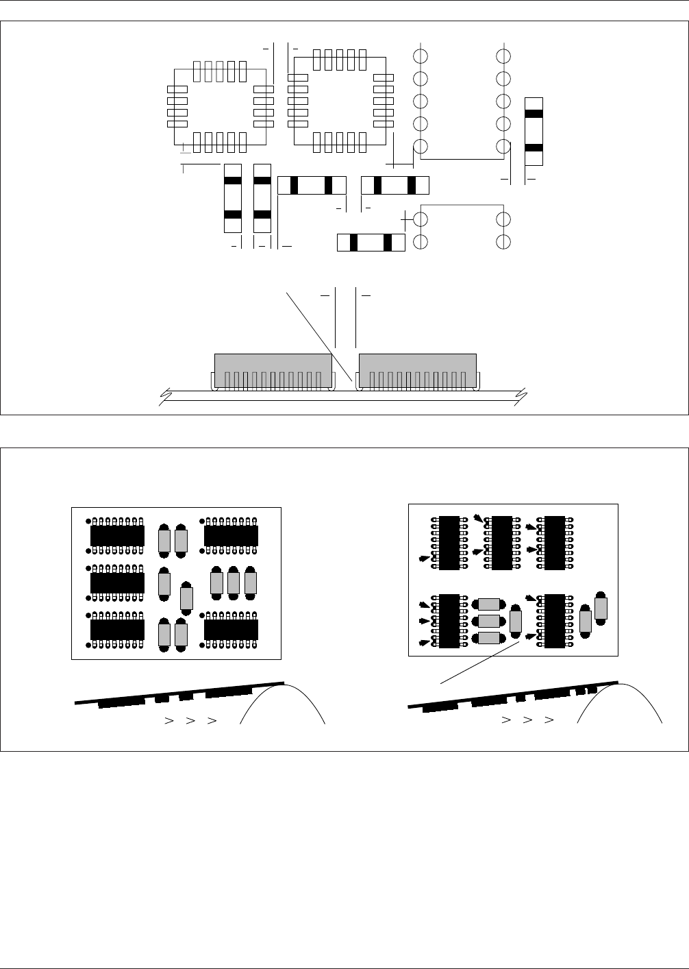
Figure 3–9 Component orientation for wave solder applications
Wave Solder For SMT
Prefered IC orientation
Rubber pads will reduce
solder bridging
Typical solder
bridge locations
▼
▼
Non Prefered IC orientation
December 1999 IPC-SM-782A
21
grid based placement rules of the THT boards. This ulti-
mately results in components being randomly placed, and
vias being even more randomly placed across the board.
Two problems created by random component placement
are a loss of uniform grid based test node accessibility and
a loss of logical, predictable routing channels on all layers
(possibly driving layer counts). In addition the accepted
international grid identified in IPC-1902 states that for new
designs the grid should be 0.5 mm, with a further subdivi-
sion being 0.05 mm. One solution to the problem is to
build CAD libraries with all component lands connected to
vias on 0.05 mm centers (or greater, based on design) to be
used for testing, routing, and rework ports. Then when
doing the component placement on the CAD system, sim-
ply place the components so that there is a minimum space
of 0.5 mm between lands, then snap the vias of the compo-
nent being placed out to the next 1.0 mm grid point. With
this procedure, all of the components should have between
0.4 mm and 0.6 mm (or an average of 0.5 mm) spacing
between the lands. From the assembly point of view, it is
easier to process a PCB which has the component centroids
on a 1.0 mm grid, with approximately equal spacing
between all of the lands across the board in both directions.
3.6.1.5 Single vs Double Sided Boards The term single
or double sided referred to one or two conductor layers on
a printed board prior to the advent of Surface Mount. Now,
however, the term single side refers to components
mounted on one side (Type 1 assembly), and the term
double refers to components mounted on both sides (Type
2 assembly) of the board. It has been observed that many
SMT designers, especially novices, are too quick to place
components on the secondary side of the PB, forcing the
assembly process to be executed twice instead of once.
Designers should concentrate on getting all components on
the primary side of the board whenever possible without
creating component spacing violations. This will result in a
lower assembly cost. If double sided placement is defi-
nitely required, then grid-based placement, although more
difficult, is even more crucial for accurate final component
placement, circuit routability, and testability. Double sided
boards using conventional SMT design rules often require
double sided, or clamshell test fixtures that are 3 to 5 times
the cost of single sided test fixtures. Grid based component
placements have been known to improve nodal accessibil-
ity as well as eliminate the need for dual sided testing.
3.6.1.6 Solder Stencil Design The solder stencil is the
primary vehicle by which solder paste is applied to the
SMT printed board. With it, the exact location and volume
of solder paste deposition is precisely controlled. The art-
work for the stencil generally consists of the component
mounting lands from the outer layers of the board with all
other circuitry deleted. The openings in the stencil should
be the same size as the lands on the board for all compo-
nents. The printed board assembler may alter the stencil
IPC-782-3-10
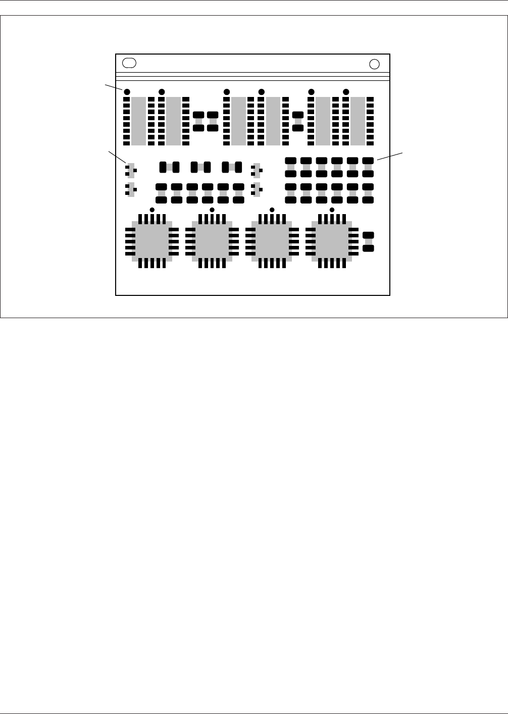
Figure 3–10 Alignment of similar components
Consistent
Orientation
PIN One I. D.
Uniform
Spacing
▼
▼
▼
PREFERRED LAYOUT FOR SMT
IPC-SM-782A December 1999
22
opening size prior to manufacturing the stencil to change
the volume of solder paste which is deposited on the lands.
3.6.1.7 Component Stand Off Height for Cleaning The
minimum component stand off height for cleaning is based
on the distance across the diagonal of the component. This
dimension implies a component surface area that may trap
contamination if care is not exercised. Table 3–7 shows the
relationship for recommended component standoff dis-
tances.
If the minimum stand off cannot be achieved, proper clean-
ing under the component may not be possible. In this case
it is recommended that a no clean flux be used.
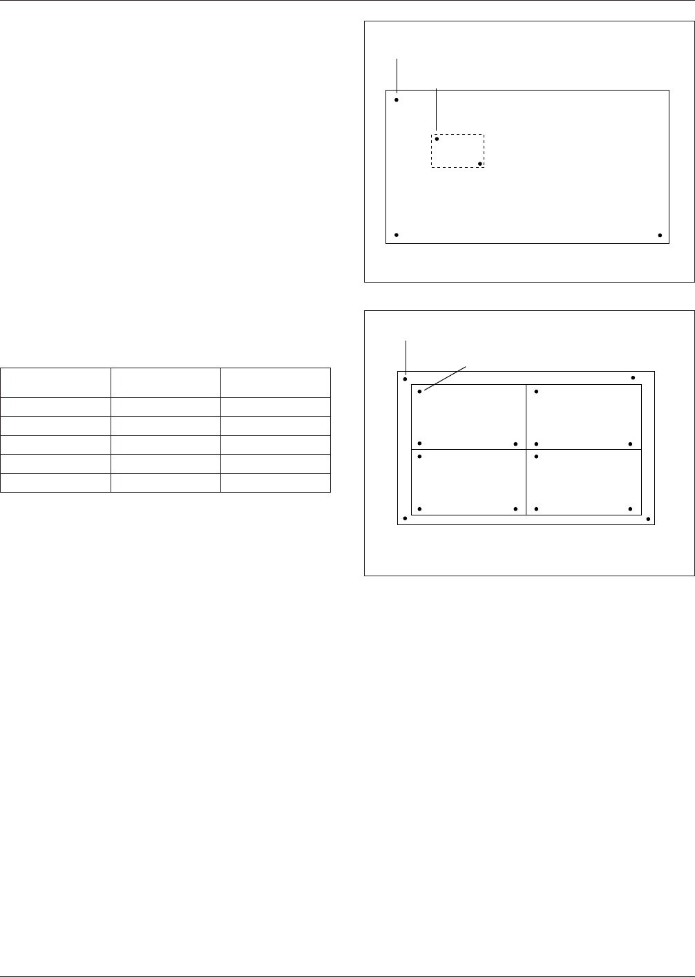
3.6.1.8 Fiducial Marks A Fiducial Mark is a printed art-
work feature which is created in the same process as the
circuit artwork. The fiducial and a circuit pattern artwork
must be etched in the same step.
The Fiducial Marks provide common measurable points for
all steps in the assembly process. This allows each piece of
equipment used for assembly to accurately locate the cir-
cuit pattern. There are two types of Fiducial Marks. These
are:
A. Global Fiducials
Fiducial marks used to locate the position of all circuit
features on an individual board. When a multi image
circuit is processed in panel form, the Global Fiducials
are referred to as Panel Fiducials when present for the
panel. (See Figures 3–11/3–12.)
B. Local Fiducials
Fiducial marks used to locate the position of an indi-
vidual component requiring more precise placement.
(See Figure 3–11.)
A minimum of two global fiducial marks is required for
correction of translational offsets (x and y position) and
rotational offsets (theta position). These should be located
diagonally opposed and as far apart as possible on the cir-
cuit or panel.
A minimum of three fiducial marks is required for correc-
tion of non linear distortions (scaling, stretch and twist).
These should be located in a triangular position as far apart
as possible on the circuit or panel.
A minimum of two local fiducial marks are required for
correction of translational offsets (x and y position) and
rotational offsets (theta position). This can be two marks
located diagonally opposed within the perimeter of the land
pattern.
If space is limited, a minimum of one local fiducial mark
may be used to correct translational offsets (x and y posi-
tion). The single fiducial should be located inside the
perimeter of the land pattern with a preference for the cen-
ter.
The minimum size for local, global or panel fiducials is 1.0
mm. Some companies have chosen a larger fiducial (up to
1.5 mm) for panel fiducials. It is a good practice to keep all
fiducials the same size.
Table 3–7 Component Stand Off
Component
Diagonal
Component
Surface Area
Component Stand
Off
< = 50 mm < = 2500 mm
2
> = 0.5 mm
<=25mm <=625mm
2
> = 0.3 mm
<=12mm <=144mm
2
> = 0.2 mm
<=6mm <=36mm
2
> = 0.1 mm
<=3mm <=9mm
2
> = 0.05 mm
IPC-782-3-11
Figure 3–11 Local/global fiducials
Global fiducial
Local fiducial
▼
▼
IPC-782-3-12
Figure 3-12 Panel/global fiducials
Panel fiducial
▼
Global fiducial
▼
December 1999 IPC-SM-782A
23