IPC-SM-782A-表面贴装焊盘图形设计标准.pdf.pdf - 第32页
3.6.1.9 Fiducial Mark Design Specifications The Sur- face Mount Equipment Manufacturers Association (SMEMA) has standardized on the design rules for fidu- cials. These rules are supported by the IPC and consist of: A. Sha…
opening size prior to manufacturing the stencil to change
the volume of solder paste which is deposited on the lands.
3.6.1.7 Component Stand Off Height for Cleaning The
minimum component stand off height for cleaning is based
on the distance across the diagonal of the component. This
dimension implies a component surface area that may trap
contamination if care is not exercised. Table 3–7 shows the
relationship for recommended component standoff dis-
tances.
If the minimum stand off cannot be achieved, proper clean-
ing under the component may not be possible. In this case
it is recommended that a no clean flux be used.
3.6.1.8 Fiducial Marks A Fiducial Mark is a printed art-
work feature which is created in the same process as the
circuit artwork. The fiducial and a circuit pattern artwork
must be etched in the same step.
The Fiducial Marks provide common measurable points for
all steps in the assembly process. This allows each piece of
equipment used for assembly to accurately locate the cir-
cuit pattern. There are two types of Fiducial Marks. These
are:
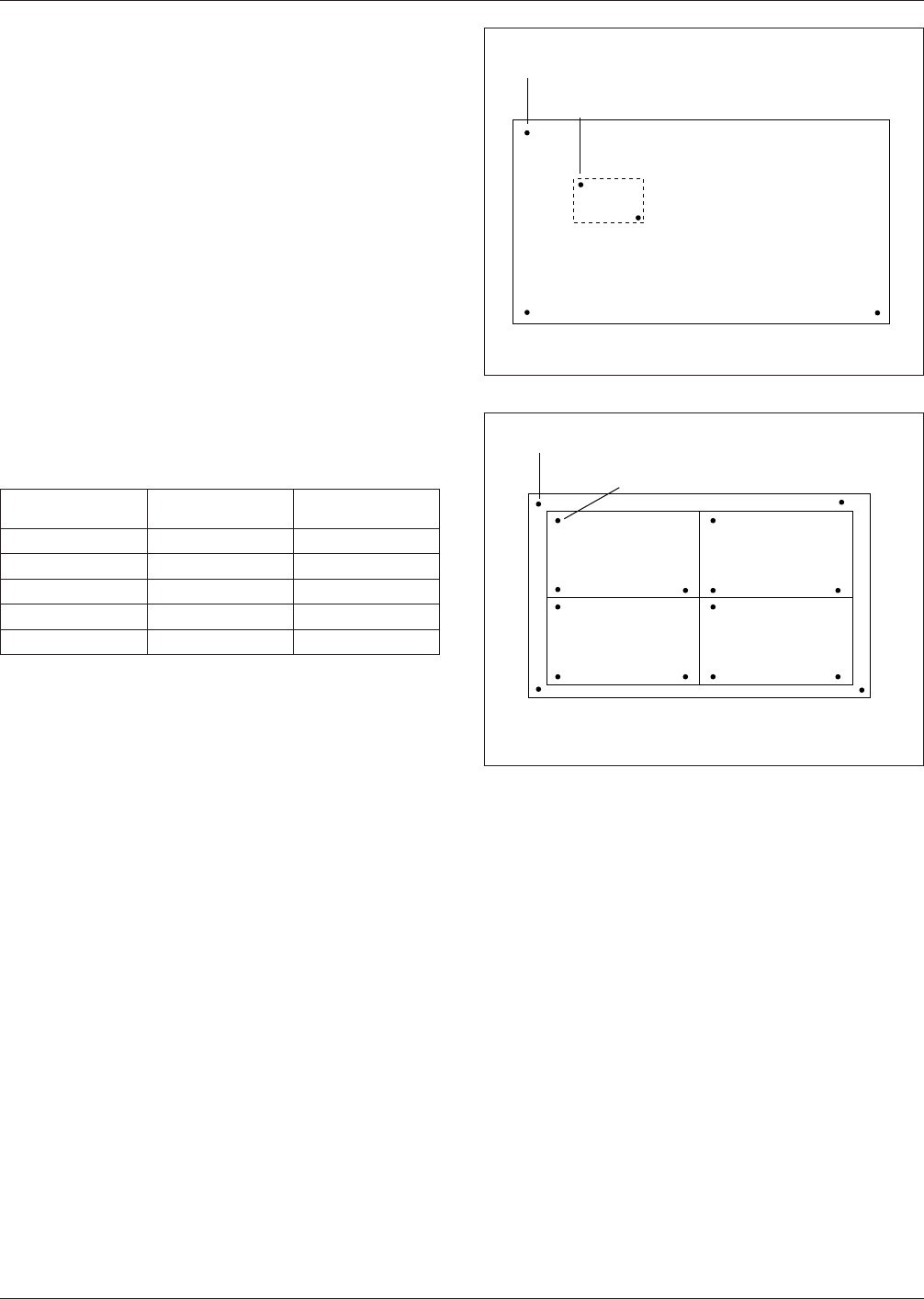
A. Global Fiducials
Fiducial marks used to locate the position of all circuit
features on an individual board. When a multi image
circuit is processed in panel form, the Global Fiducials
are referred to as Panel Fiducials when present for the
panel. (See Figures 3–11/3–12.)
B. Local Fiducials
Fiducial marks used to locate the position of an indi-
vidual component requiring more precise placement.
(See Figure 3–11.)
A minimum of two global fiducial marks is required for
correction of translational offsets (x and y position) and
rotational offsets (theta position). These should be located
diagonally opposed and as far apart as possible on the cir-
cuit or panel.
A minimum of three fiducial marks is required for correc-
tion of non linear distortions (scaling, stretch and twist).
These should be located in a triangular position as far apart
as possible on the circuit or panel.
A minimum of two local fiducial marks are required for
correction of translational offsets (x and y position) and
rotational offsets (theta position). This can be two marks
located diagonally opposed within the perimeter of the land
pattern.
If space is limited, a minimum of one local fiducial mark
may be used to correct translational offsets (x and y posi-
tion). The single fiducial should be located inside the
perimeter of the land pattern with a preference for the cen-
ter.
The minimum size for local, global or panel fiducials is 1.0
mm. Some companies have chosen a larger fiducial (up to
1.5 mm) for panel fiducials. It is a good practice to keep all
fiducials the same size.
Table 3–7 Component Stand Off
Component
Diagonal
Component
Surface Area
Component Stand
Off
< = 50 mm < = 2500 mm
2
> = 0.5 mm
<=25mm <=625mm
2
> = 0.3 mm
<=12mm <=144mm
2
> = 0.2 mm
<=6mm <=36mm
2
> = 0.1 mm
<=3mm <=9mm
2
> = 0.05 mm
IPC-782-3-11
Figure 3–11 Local/global fiducials
Global fiducial
Local fiducial
▼
▼
IPC-782-3-12
Figure 3-12 Panel/global fiducials
Panel fiducial
▼
Global fiducial
▼
December 1999 IPC-SM-782A
23
3.6.1.9 Fiducial Mark Design Specifications The Sur-
face Mount Equipment Manufacturers Association
(SMEMA) has standardized on the design rules for fidu-
cials. These rules are supported by the IPC and consist of:
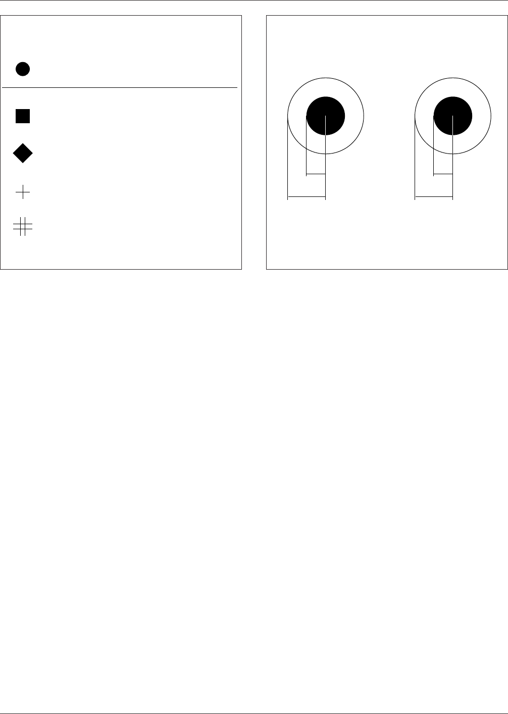
A. Shape
The optimum fiducial mark is a solid filled circle. See
Figure 3–13.
B. Size
The minimum diameter of the fiducial mark is 1 mm
[0.040 in]. The maximum diameter of the mark is 3
mm [0.120 in]. Fiducial marks should not vary in size
on the same PB more than 25 microns [0.001 in].
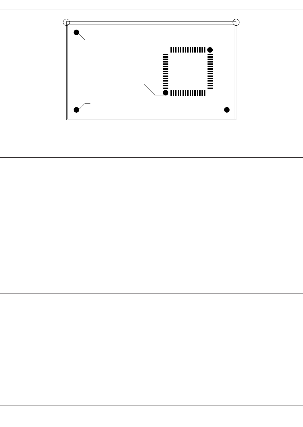
C. Clearance
A clear area devoid of any other circuit features or
markings shall exist around the fiducial mark. The size
of the clear area shall be equal to the radius of the
mark. A preferred clearance around the mark is equal
to the mark diameter. (See Figure 3–14)
D. Material
The fiducial may be bare copper, bare copper protected
by a clear anti oxidation coating, nickel or tin plated,
or solder coated (hot air leveled).
The preferred thickness of plating or solder coating is
0.005 mm to 0.010 mm [0.0002 to 0.0004 in]. Solder
coating should never exceed 0.025 mm [0.001 in].
If solder mask is used, it should not cover the fiducial
or the clearance area. It should be noted that oxidation
of a fiducial mark’s surface may degrade its readabil-
ity.
E. Flatness
The flatness of the surface of the fiducial mark should
be within 0.015 mm [0.0006 in].
F. Edge Clearance
The fiducial shall be located no closer to the PB edge
than the sum of 4.75 mm [0.187 in] (SMEMA Standard
Transport Clearance) and the minimum fiducial clear-
ance required.
G. Contrast
Best performance is achieved when a consistent high
contrast is present between the fiducial mark and the
PB base material.
It is good design practice to locate global or panel fiducials
in a three point grid based datum system as shown in Fig-
ure 3–15. The first fiducial is located at the 0,0 location.
The second and third fiducials are located in the X and Y
directions from 0,0 in the positive quadrant. The global
fiducials should be located on the top and bottom layers of
all printed boards that contain Surface Mount as well as
Through Hole components since even Through Hole
assembly systems are beginning to utilize vision alignment
systems.
All Fine Pitch components should have two local fiducials
system designed into the component land pattern to insure
that enough fiducials are available every time the compo-
nent is placed, removed and/or replaced on the board. All
fiducials should have a soldermask opening large enough to
keep the optical target absolutely free of soldermask. If
IPC-782-3-13
Figure 3-13 Fiducial types for vision systems
Solid round dot typically 1.5mm Dia.
Preferred
Solid square typically 2.0mm on a side
Solid diamond typically 2.0mm on a side
Single cross hair typically 2.0mm high
Double cross hair typically 2.0mm high
Other
IPC-782-3-14
Figure 3-14 Fiducial clearance requirements
R
2R
Clearance
R
3R
Clearance
Minimum Preferred
▼
▼
▼
▼
▼
▼
▼
▼
IPC-SM-782A December 1999
24
soldermask should get onto the optical target, some vision
alignment systems may be rendered useless due to insuffi-
cient contrast at the target site.
The internal layer background for all fiducials must be the
same. That is, if solid copper planes are retained under
fiducials in the layer below the surface layer, all fiducials
must have copper retained. If copper is clear under one
fiducial, all must be clear.
3.6.2 Conductors
3.6.2.1 Conductor Width & Clearances
Increased com-
ponent density on SMT designs has mandated the use of
thinner conductor density and clearance between conduc-
tors with increased PB layer counts requiring the use of
more vias to make the necessary connections between the
additional layers. Figure 3–16 shows the effects of SMT
and Fine Pitch Technology (FPT) on printed board geom-
etries.
Conductor width/clearances of 0.15 mm [0.006 in] have
become commonplace today, and have basically replaced
the 0.3 mm [0.012 in] line/ space as a commonly used
geometry (see Figure 3–17). As more fine pitch (including
Tape Automated Bonding) devices are used on printed
boards, the 0.125 mm [0.005 in] geometry may be used in
more SMT boards to reduce layer counts. Figure 3–18
IPC-782-3-15
Figure 3–15 Fiducial locations on a printed circuit board
Locate all fiducials and tooling holes on the appropriate grid.
Locate fiducials on both primary and secondary side of board.
Standard tooling hole diameters: 2.4mm, 2.8mm, 3.2mm
Global fiducials should be 5.0mm Min from board edges.
Global fiducials
0
/0 Point of origin
Fine
Pitch
Component
▼
▼
▼
Local fiducials
IPC-782-3-16
Figure 3–16 Packaging and geometries
GEOMETRY
PIN COUNTS
PLACEMENT TOLERANCE
CONDUCTORS/CLEARANCE
LANDS
HOLES
ANNULAR RING
8 TO 64
.25mm
.3mm
1.5mm
1.0mm
.25mm
8 TO 124
0.125mm
0.15mm
0.75mm
0.4mm
0.2mm
84 TO 244
0.05mm
0.125mm
0.63mm
0.40mm
0.125mm
2.54mm Pitch 1.25mm Pitch 0.63mm Pitch
December 1999 IPC-SM-782A
25