IPC-SM-782A-表面贴装焊盘图形设计标准.pdf.pdf - 第34页
shows a grid routing analysis with vias on 1.0 mm [0.050 in] centers. On the left side are listed the routing grids with the actual routing channels denoted by solid triangular points. It can be seen that with SMT geomet…
soldermask should get onto the optical target, some vision
alignment systems may be rendered useless due to insuffi-
cient contrast at the target site.
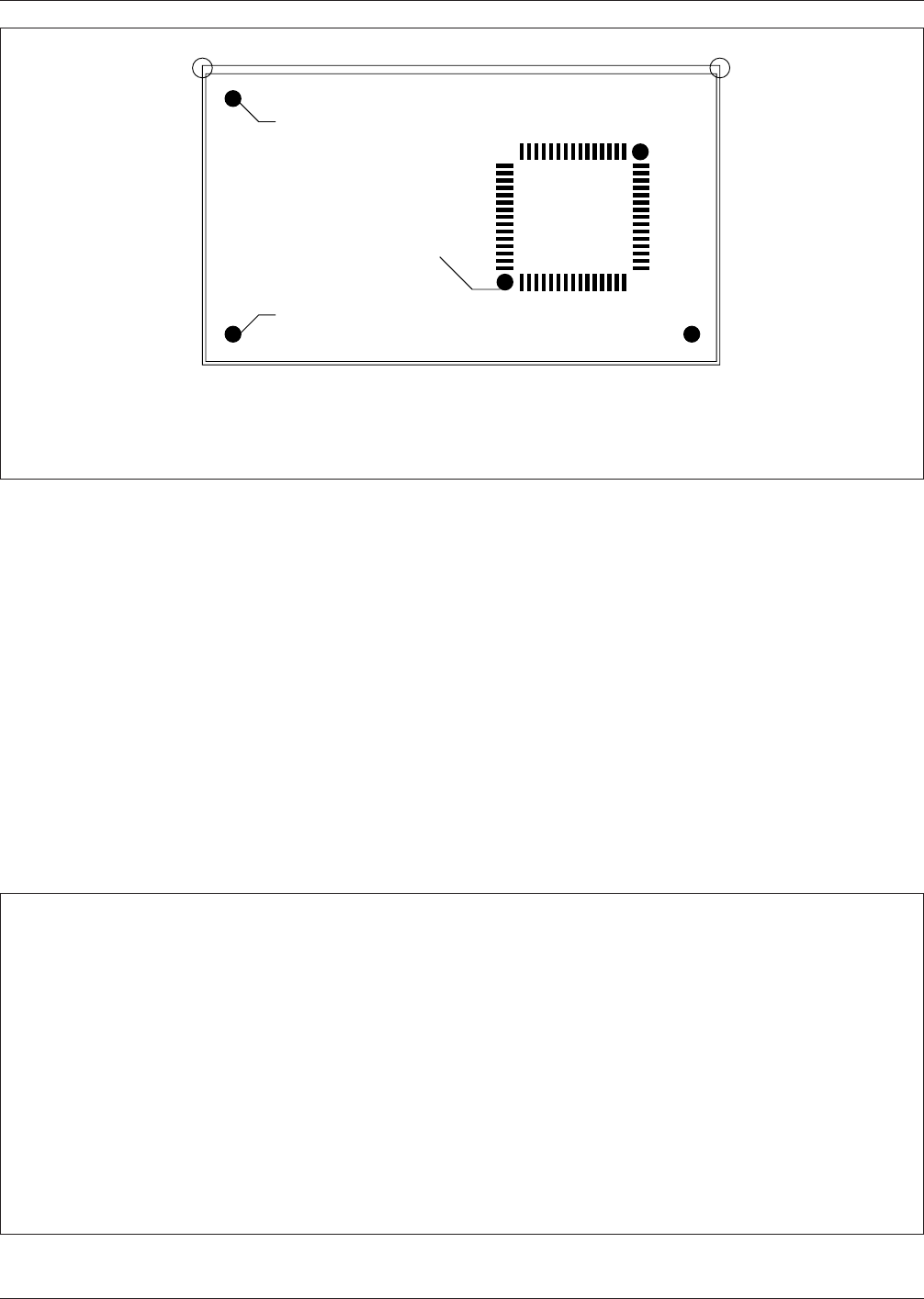
The internal layer background for all fiducials must be the
same. That is, if solid copper planes are retained under
fiducials in the layer below the surface layer, all fiducials
must have copper retained. If copper is clear under one
fiducial, all must be clear.
3.6.2 Conductors
3.6.2.1 Conductor Width & Clearances
Increased com-
ponent density on SMT designs has mandated the use of
thinner conductor density and clearance between conduc-
tors with increased PB layer counts requiring the use of
more vias to make the necessary connections between the
additional layers. Figure 3–16 shows the effects of SMT
and Fine Pitch Technology (FPT) on printed board geom-
etries.
Conductor width/clearances of 0.15 mm [0.006 in] have
become commonplace today, and have basically replaced
the 0.3 mm [0.012 in] line/ space as a commonly used
geometry (see Figure 3–17). As more fine pitch (including
Tape Automated Bonding) devices are used on printed
boards, the 0.125 mm [0.005 in] geometry may be used in
more SMT boards to reduce layer counts. Figure 3–18
IPC-782-3-15
Figure 3–15 Fiducial locations on a printed circuit board
Locate all fiducials and tooling holes on the appropriate grid.
Locate fiducials on both primary and secondary side of board.
Standard tooling hole diameters: 2.4mm, 2.8mm, 3.2mm
Global fiducials should be 5.0mm Min from board edges.
Global fiducials
0
/0 Point of origin
Fine
Pitch
Component
▼
▼
▼
Local fiducials
IPC-782-3-16
Figure 3–16 Packaging and geometries
GEOMETRY
PIN COUNTS
PLACEMENT TOLERANCE
CONDUCTORS/CLEARANCE
LANDS
HOLES
ANNULAR RING
8 TO 64
.25mm
.3mm
1.5mm
1.0mm
.25mm
8 TO 124
0.125mm
0.15mm
0.75mm
0.4mm
0.2mm
84 TO 244
0.05mm
0.125mm
0.63mm
0.40mm
0.125mm
2.54mm Pitch 1.25mm Pitch 0.63mm Pitch
December 1999 IPC-SM-782A
25
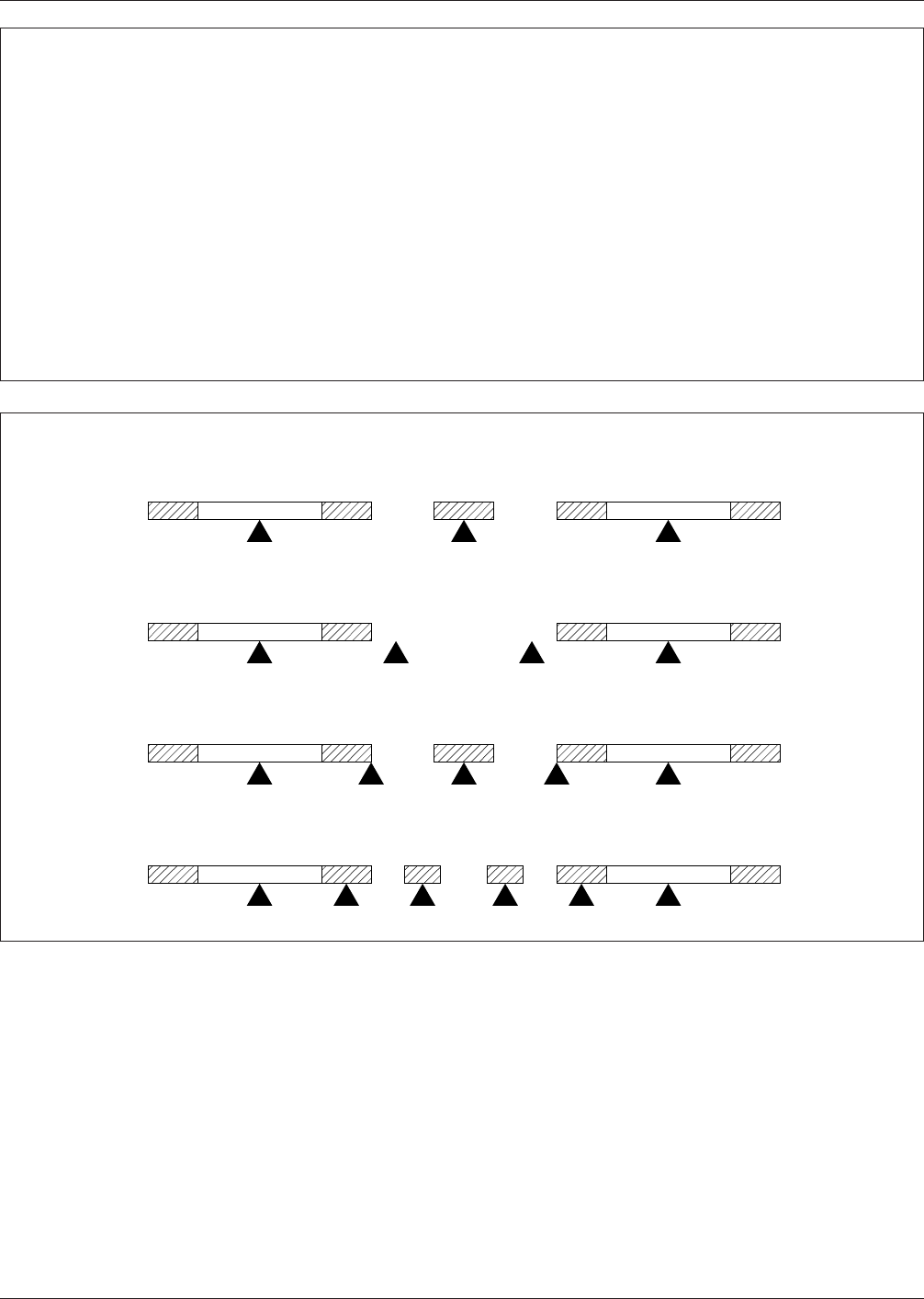
shows a grid routing analysis with vias on 1.0 mm [0.050
in] centers. On the left side are listed the routing grids with
the actual routing channels denoted by solid triangular
points. It can be seen that with SMT geometry of vias
placed on 1.0 mm [0.040 in] centers, there is one routing
channel between lands using a 0.3 mm [0.012 in] grid with
0.15 mm [0.006 in] conductor width/clearances. The bot-
tom routing grid of 0.25 mm [0.010 in] with 0.125 mm
[0.005 in] has two routing channels between vias.
3.6.2.2 Surface Conductors Wide conductors connect-
ing to a land area can act as a solder thief by drawing sol-
der away from the land and down the conductor. Further-
more, if the conductor goes to a via which is connected to
an inner layer power or ground plane, the wide conductor
may act as a heat sink and draw heat away from the land/
lead area during reflow solder resulting in a cold solder
joint.
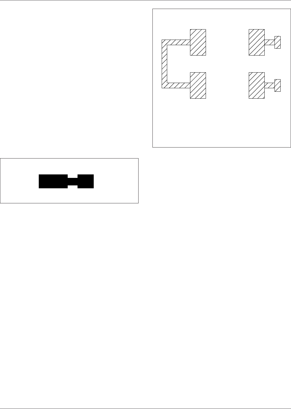
A. Narrow the conductor as it enters the land area. Maxi-
mum conductor width should be 0.25 mm [0.010 in]
(see Figure 3–19). The minimum conductor length
should be 0.50 mm [0.020 in]. This neckdown provides
an effective solder restriction, and may eliminate the
IPC-782-3-17
Figure 3–17 Surface mount conductor widths/clearances vs. routing grids
ROUTING GRIDS
.63mm
0.5mm
0.4mm
0.3mm
0.25mm
MANUFACTURING
ALLOWANCE
0.1mm
0.1mm
0.05mm
0.05mm
0.05mm
MINIMUM
CONDUCTORS/CLEARANCE
0.3/0.2mm
0.2/0.2mm
0.2/0.15mm
0.15/0.1mm
0.10/0.10mm
IPC-782-3-18
Figure 3–18 Section view of multilayer board with vias on 1.0 mm [0.040 in] centers
0.5mm SQ Land MIN 0.25mm DRILL
.5mm
GRID
.33mm
GRID
.25mm
GRID
.20mm
GRID
One
Track
Zero
Track
One
Track
Two
Track
.16mm .16mm
.18mm
.18mm
.16mm .16mm
.125mm .125mm
.125mm .125mm.125mm
IPC-SM-782A December 1999
26
need to use a soldermask to prevent the migration of
solder away from the component land.
B. Routing conductors into the lands as shown in Figures
3–20, 3–21 may restrict discrete component movement
during reflow soldering. In the case of active IC’s this
routing geometry will allow the designer to use the
same library shape for surface routing or pad cap (no
surface routing) printed board configuration. Addition-
ally, using this generic library shape allows ease of
switching between the two configurations midstream in
the design process without changing or editing compo-
nent libraries. In either case, 100% test node access is
retained. If wider conductors are required, the via land
size may be decreased accordingly to allow sufficient
spacing between the conductor and the land.
C. Use solder mask over bare copper (SMOBC) or copper
that has had the solder plating selectively removed.
The solder mask and bare copper provide an effective
barrier to solder migration. This may provide sufficient
protection even if options A and B are not possible.
3.6.2.3 Inner Layer Conductors The use of 0.2 mm
[0.008 in] conductors and clearance often drives layer
counts up because there is no routing channel available
between vias on 1.27 mm [0.050 in] centers. It is for this
reason that there is an increased usage of the conductors on
internal layers at or less than 0.15 mm [0.006 in] for SMT
designs, and 0.125 mm [0.005 in] conductors and clear-
ances for designs with heavy usage of FPT. Figure 3–22
and 3–23 show the number of routing channels available
between lands using the 0.15 and 0.125 mm [0.006 and
0.005 in] geometries. Since conductor width control is
much more difficult to maintain on outer layers of the PB,
it is better to keep the small geometries on the inner layers
of a multilayer printed board. Doing so may reduce the
need for soldermask and dramatically improve printed
board fabrication yields. Generally, the option of using
smaller geometries is driven by the need to reduce layer
counts. Decreasing layer counts may reduce the overall
board thickness and improve the aspect ratio for small hole
drilling.
3.6.3 Via Location Guidelines
3.6.3.1 Via Holes
Size of the via holes should be
selected based upon the printed board thickness vs. hole
diameter or aspect ratio limits as defined by printed board
fabricator. In addition, specific via lands and holes can be
accessed for automatic in-circuit test (ICT). See 5.3.1. Fig-
ure 3–24 shows the land pattern-to-via relationships.
3.6.3.2 Vias and Land Pattern Separation Vias are
plated-through holes for example 0.63 mm to 1.0 mm
[0.025 to 0.040 in] diameter lands. They must be located
away from the component lands to prevent solder migra-
tion off the component land during reflow soldering. This
migration will cause insufficient solder fillets on compo-
nents. (Solder drain) The solder migration can be restricted
by providing a narrow bridge between the land area and the
via or prevented by using the soldermask over bare copper
circuitry. (See Figures 3–19 and 3–20.)
The relationship for mounting land and via locations
should consider the conductor routing requirements. Figure
3–25 provides several examples of via positioning con-
cepts.
Specifying tented or filled vias will also reduce solder
migration on assemblies manufactured with a solder reflow
process. Filled or tented vias also take care of potential flux
entrapment problems under components and are highly
desirable for attaining good vacuum seal during in-circuit
bed-of-nails testing. Tenting is done with a dry film type of
soldermask, or the via may be filled with a resin prior to
liquid soldermask application.
3.6.3.3 Vias Under Components If the assembly is to be
wave soldered, via holes underneath zero clearance compo-
nents on the primary side should be avoided on boards
unless tented with soldermask. During wave soldering of
the assembly, flux may potentially become trapped under
IPC-782-3-19
Figure 3–19 Narrowed conductor
IPC-782-3-20
Figure 3–20 Conductor routing
Conductors routing
away from lands
Conductors routing
to vias
December 1999 IPC-SM-782A
27