IPC-SM-782A-表面贴装焊盘图形设计标准.pdf.pdf - 第57页
6.1 General Considerations P&I Structures vary from basic printed wiring boards to very sophisticated supporting-core structures. However , some selection crite- ria are common to all structures. T o aid in the selec…

this critical parameter. Also, the functional or system test
must be capable of at least detecting any fault (even if
detection means that the test simply won’t run). A possibil-
ity in this case is to discard faulty product rather than diag-
nose it (of course this must be included in the cost analy-
sis).
Another option is that the faulty unit can be debugged by a
test technician, but this may also be an expensive proposi-
tion, as faults in unscreened boards (no shorts or defects
testing) can be very time consuming to diagnose, even for
an experienced technician.
5.6 Clam Shell Fixtures Impact Probing the printed
board from both sides requires a ‘‘clam shell’’ type of fix-
ture. These are expensive, take a long time to fabricate,
require larger test lands on the primary side to protect
against registration problems due to tolerance stackups.
These typically would be 1.25 mm [0.050 in]. This uses up
excessive real estate. Also, ‘‘clam shell’’ fixtures tend to
lose their registration and are difficult to maintain.
5.7 Printed Board Test Characteristics
5.7.1 General Land Pattern Considerations
Circuit
design for testability refers to the practice of insuring
observability and controllability of all nodes by not hard
wiring presets or clears, and providing means to break any
feedback loops.
Design for testability is as much a part of the schematic
design process as it is a part of the board layout process.
Due to the extensive use of ATE to test SMT printed
boards, the printed board designer needs to follow the pre-
vious rules to provide test node points on the printed board.
As SMT Design for Test advances with technology, it is
mandatory that continuous improvements to the test pro-
cess be developed and implemented through Concurrent
Engineering.
Ideally, the printed board would have 100% of the nodes
accounted for on the secondary side. See Figure 5–2.
In-Circuit Testers must have access to at least one node per
net. All test lands would be on 2.5 mm [0.100 in] or 1.25
mm [0.050 in] minimum spacings. This allows for the least
costly, most reliable, and fastest manufacture of the test
fixture.
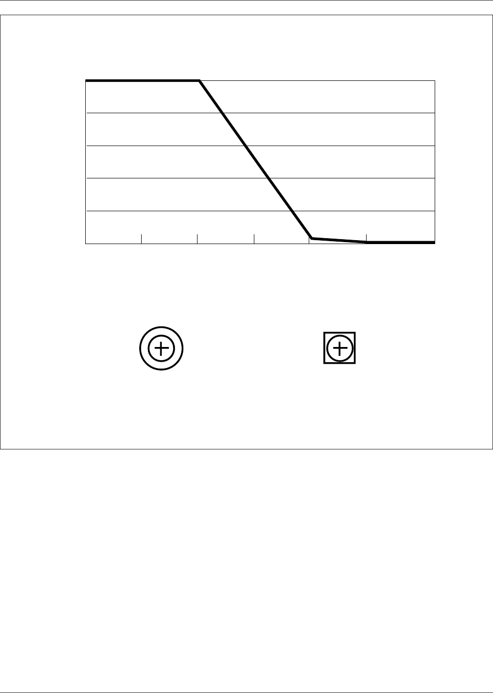
Lands or vias should be 0.9 to 1.0 mm [0.035 to 0.040
inch] for probing. This via size will ensure less than three
misses per 1000 probes. As land sizes decrease, misses
increase dramatically as shown in Figure 5–2. The use of
square via lands will provide a larger target zone for the
test probe to contact. Figure 5–2 demonstrates the addi-
tional area that the square land offers. Using the square
land, the size may be reduced to 0.8 mm [0.032 in] to
increase the spacing between lands if necessary.
The drawbacks to the 1.25 mm grid based test lands are:
1.25 mm [0.050 in] spring probes are more expensive than
the cost of 2.5 mm [0.100 in] spring probes. They do not
hold up as well in high volume production and the fixture
takes longer to manufacture. Also, any vias used as test
points should be solder filled for better contact and
increased probe life.
5.7.2 Design for Test Parameters The following other
considerations are important to the general land pattern
design that should be incorporated into the printed board.
• Unplated tooling holes should be available on diagonal
corners of the printed board.
• Test lands should be 2.5 mm [0.100 in] minimum from
the edge of the printed board to facilitate gasketing on
vacuum fixtures.
• When using vias for test points, caution should be taken
to insure that signal quality is not degraded at the
expense of testing capability.
• Test lands should be 0.63 mm [0.025 in] minimum from
mounting land areas.
• It is useful to mark the test vias and lands on an assem-
bly drawing in event of the need to modify the circuit
topology. Changes made without moving test lands,
avoid fixture modification, saving cost and time.
• When possible, provide numerous test lands for power
and ground.
• When possible, provide test lands for all unused gates.
Free running gates sometimes cause instability during
in-circuit testing. This will provide a means of ground-
ing these spurious signals.
• It is sometimes desirable to provide drive and sense
nodes test lands to perform 6-wire bridge measurements
during in-circuit test. Direction for this should come
from test engineering.
• Caution should be taken when mounting components on
the secondary side to avoid covering a via that is a des-
ignated test land. Also, if a via is too close to any
component, damage may result to the component or fix-
ture during probing. See Figure 5–3.
6.0 PACKAGING AND INTERCONNECTING STRUCTURE
TYPES
The selection of a packaging and interconnecting structure
for surface mounting applications is important for optimum
thermal, mechanical and electrical systems reliability. Each
candidate structure has a set of properties with particular
advantages and disadvantages when compared to others
(see Table 6–1).
It is probable that no one packaging and interconnecting
structure or printed board will satisfy all of the needs of the
application. Therefore, a compromise of properties should
be sought that offers the best ‘‘tailoring’’ for component
attachment and circuit reliability.
IPC-SM-782A December 1999
48
6.1 General Considerations P&I Structures vary from
basic printed wiring boards to very sophisticated
supporting-core structures. However, some selection crite-
ria are common to all structures. To aid in the selection
process, Table 6–2 lists design parameters and material
properties which affect system performance, regardless of
P&IS type. Also, Table 6–3 lists the properties of the mate-
rials most-common for these applications.
6.1.1 Categories In general, a P&I structure will fit into
one of four basic categories of construction: organic base
material, non-organic base material, supporting plane, and
constraining core.
6.1.2 Thermal Expansion Mismatch A primary concern
of surface mounted leadless parts is the thermal expansion
mismatch between the leadless part and the P&I structure.
This mismatch will fracture solder joint interconnections if
the assembly is subjected to thermal shock, thermal
cycling, power cycling and high operating temperatures.
The number of fatigue cycles before solder joint failure
depends on the thermal expansion mismatch between the
part and the P&I structure, the temperature range over
which the assembly must operate, the solder joint thick-
ness, the size of the part and the power cycling. For
example, power cycling may cause an undesirable thermal
expansion mismatch if a significant temperature difference
exists between a chip carrier and the P&I structure.
IPC-782-5-2
Figure 5–2 General relationship between test contact size and test probe misses
Probability of at Least One Miss
Test/Via Probe Contact Size
100%
80%
60%
40%
20%
0%
0.25mm 0.35mm 0.5mm 0.6mm
Diameter
0.75mm 0.9mm 1.0mm
1.0mm Dia
[0.04"]
0.9mm Square
[.036"]
**
*
*
*
December 1999 IPC-SM-782A
49

The acceptable number of cycles can be increased by
reducing the thermal expansion mismatch, reducing the
temperature gradient, increasing the solder joint height,
using the smallest physical size part where possible, and by
optimizing the thermal path between the part and P&I
structure. The overall systems operating requirements for
each class of hardware determines the acceptable number
of cycles.
6.2 Organic-Base Material P&IS Organic-base materials
work best with leaded chip carriers. With leadless chip car-
riers, however, the thermal expansion mismatch between
package and substrate can cause problems. Also, flatness,
rigidity, and thermal conductivity requirements may limit
their use. Finally, you must pay attention to package size,
I/O count, thermal cycling stability, maximum operating
temperature and solder joint compliance.
6.3 Non-Organic Base Materials Non-organic base
materials typically used with thick-or thin-film technology
are also ideally suited for leaded and leadless chip carrier
designs. They can incorporate thick- or thin-film resistors
directly on the P&I structure and buried capacitor layers
that increase density and improve reliability. However,
repairability of the P&I structure is limited. Ceramic mate-
rials, usually alumina, appear ideal for P&I structure with
leadless ceramic chip carriers because of their relatively-
high thermal conductivity (see Table 6–3) and the coeffi-
cient of thermal expansion (CTE) match. Unfortunately, the
P&I structure is limited to approximately 22,600 sq. mm.
[35 square inches]. However, the evolving use of these
materials with non-noble metals, such as copper, has
attracted both military and commercial applications.
Ceramic P&I structures currently have three applications:
ceramic hybrid circuits, ceramic multichip modules
(MCM-L) and ceramic printed boards.
6.4 Supporting-Plane P&I Structures Supporting metal-
lic or non-metallic planes can be used with conventional
printed boards or with custom processing to enhance P&IS
properties. Depending on the results desired, the supporting
plane can be electrically-functional or not and can also
serve as a structure stiffener, heatsink and/or CTE con-
straint.
High-density, sequentially-processed, multilayer P&I struc-
tures are available with organic dielectrics of specific thick-
ness, ultrafine conductors, and solid plated vias for layer-
to-layer interconnections with thermal lands for heat trans-
fer, all connected to a low-CTE metal support heatsink.
Thus, this technology combines laminating materials,
chemical processing, photolithography, metallurgy, and
unique thermal transfer innovations, such that it is also
appropriate for mounting and interconnecting bare inte-
grated circuit chips.
The major advantage of this system is that the vias can be
as small as 0.20 mm [0.005 inches] square and conductor
widths can range from 0.12 to 0.20 mm [0.003 to 0.005
inches] for high interconnection density. Thus, most appli-
cations can be satisfied with two signal layers with addi-
tional layers for power and ground.
Discrete-wire P&I structures have been developed specifi-
cally for use with surface mounted components, as shown
in Figure 5–3. These structures are usually built with a
low-expansion metal support plane that also offers good
heat dissipation.
The interconnections are made by discrete 0.06 mm
[0.0025 inch] diameter insulated copper wires precisely
placed on a 0.03 mm [inch] grid by numerically-controlled
IPC-782-5-3
Figure 5–3 Test probe feature distance from component
Component
Height
▼
▼
▼
Free
Area
6.5mm [0.255"] height
> 5.0mm
[0.20"] Min.
Test
Pad
5.0mm [0.20"]
Tall Component
Free area
▼
Diagram Showing Free Area around Test Pad
for Components Greater than 6.5mm in Height
▼
Test Pad
IPC-SM-782A December 1999
50