IPC-SM-782A-表面贴装焊盘图形设计标准.pdf.pdf - 第72页
4.0 COMPONENT DIMENSIONS Figure 2 provides the component dimensions for chip resistors. mm [in] Component Identifier LS W T H min max min max min max min max max 1005 [0402] 1.00 1.10 0.40 0.70 0.48 0.60 0.10 0.30 0.40 16…
1.0 SCOPE
Microminiature leadless devices are available to the circuit
designer in rectangular form for discrete components such as
chip resistors.
This subsection provides the component and land pattern
dimensions for chip resistors, along with an analysis of toler-
ance and solder joint assumptions used to arrive at the land
pattern dimensions. Basic construction of the chip resistor is
also covered.
2.0 APPLICABLE DOCUMENTS
See Section 8.0 for documents applicable to the subsections.
3.0 COMPONENT DESCRIPTIONS
A variety of values exist for resistors. The following sections
describe the most common types.
3.1 Basic Construction The resistive material is applied to
a ceramic substrate and terminated symmetrically at both
ends with a ‘‘wrap around’’ metal U-shaped band. The resis-
tive material is face-up, thus trimming to close tolerances is
possible. Since most equipment uses a vacuum-type pickup
head, it is important that the surface of the resistor is made flat
after trimming, otherwise vacuum pickup might be difficult.
See Figure 1.
3.1.1 Termination Materials End terminations should be
solder coated with a tin/lead alloy. The solder should contain
between 58 to 68% tin. Solder may be applied to the termi-
nation by hot dipping or by plating from solution. Plated sol-
der terminations should be subjected to a post-plating reflow
operation to fuse the solder. The tin/lead finish should be at
least 0.0075 mm [0.0003 in.] thick.
The termination shall be symmetrical, and shall not have nod-
ules lumps, protrusions, etc., that compromise the symmetry
or dimensional tolerances of the part. The end termination
shall cover the ends of the components, and shall extend out
to the top and bottom of the component.
Solder finish applied over precious metal electrodes shall have
a diffusion-barrier layer between the electrode metalization
and the solder finish. The barrier layer should be nickel or an
equivalent diffusion barrier, and should be at least 0.00125
mm [0.00005 in] thick.
3.1.2 Marking Resistors equal to or larger than 2012
[0805] are labeled. Resistors smaller than 1608 [0603] are
generally unlabeled.
3.1.3 Carrier Package Format Bulk rods, 8 mm tape/4
mm pitch is preferred for best handling. Tape and reel speci-
fications provide additional requirements.
3.1.4 Resistance to Soldering Parts should be capable of
withstanding five cycles through a standard reflow system
operating at 215°C. Each cycle shall consist of 60 seconds
exposure at 215°C. Parts must also be capable of withstand-
ing a minimum of 10 seconds immersion in molten solder at
260°C.
IPC-782-8-1-1
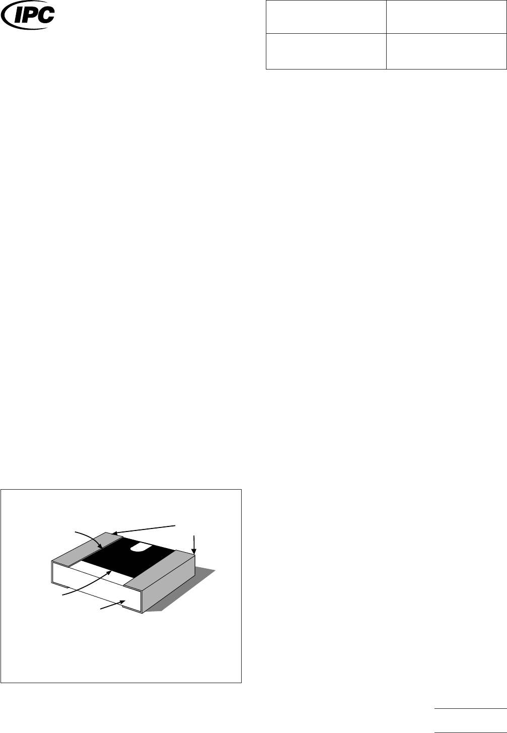
Figure 1 Chip resistor construction
Resistor
Alumina Chip
Platinum-silver
Wrap-around
termination
Wire Bond Construction
Glass
Passivation
IPC-SM-782
Surface Mount Design
and Land Pattern Standard
Date
5/96
Section
8.1
Revision
A
Subject
Chip Resistors
Page1of4
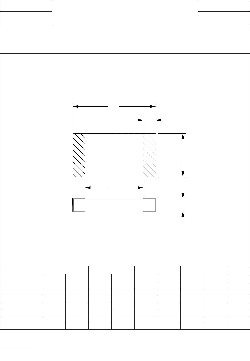
4.0 COMPONENT DIMENSIONS
Figure 2 provides the component dimensions for chip
resistors.
mm [in]
Component
Identifier
LSWTH
min max min max min max min max max
1005 [0402] 1.00 1.10 0.40 0.70 0.48 0.60 0.10 0.30 0.40
1608 [0603] 1.50 1.70 0.70 1.11 0.70 0.95 0.15 0.40 0.60
2012 [0805] 1.85 2.15 0.55 1.32 1.10 1.40 0.15 0.65 0.65
3216 [1206] 3.05 3.35 1.55 2.32 1.45 1.75 0.25 0.75 0.71
3225 [1210] 3.05 3.35 1.55 2.32 2.34 2.64 0.25 0.75 0.71
5025 [2010] 4.85 5.15 3.15 3.92 2.35 2.65 0.35 0.85 0.71
6332 [2512] 6.15 6.45 4.45 5.22 3.05 3.35 0.35 0.85 0.71
Figure 2 Chip resistor component dimensions
L
S
T
W
H
IPC-782-8-1-2
IPC-SM-782
Subject
Chip Resistors
Date
5/96
Section
8.1
Revision
A
Page2of4
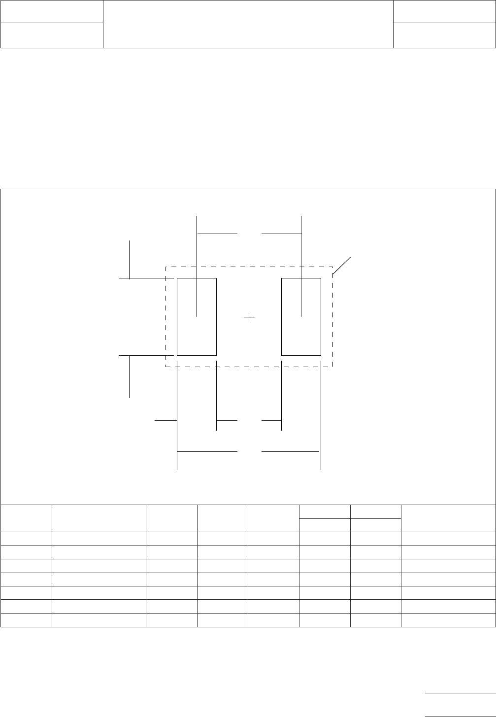
5.0 LAND PATTERN DIMENSIONS
Figure 3 provides the land pattern dimensions for chip resis-
tors. These numbers represent industry consensus on the
best dimensions based on empirical knowledge of fabricated
land patterns.
In the table, the dimensions shown are at maximum material
condition (MMC). The least material condition (LMC) should
not exceed the fabrication (F) allowance shown on page 4.
The LMC and the MMC provide the limits for each dimension.
The dotted line in Figure 3 shows the grid placement court-
yard which is the area required to place land patterns and
their respective components in adjacent proximity without
interference or shorting. Numbers in the table represent the
number of grid elements (each element is 0.5 by 0.5 mm) in
accordance with the international grid detailed in IEC publica-
tion 97.
RLP No.
Component Identifier
(mm) [in.] Z (mm) G (mm) X (mm)
Y (mm) C (mm)
Placement Grid
(No. of Grid Elements)
ref ref
100A 1005 [0402] 2.20 0.40 0.70 0.90 1.30 2x6
101A 1608 [0603] 2.80 0.60 1.00 1.10 1.70 4x6
102A 2012 [0805]* 3.20 0.60 1.50 1.30 1.90 4x8
103A 3216 [1206]* 4.40 1.20 1.80 1.60 2.80 4x10
104A 3225 [1210]* 4.40 1.20 2.70 1.60 2.80 6x10
105A 5025 [2010]* 6.20 2.60 2.70 1.80 4.40 6x14
106A 6332 [2512]* 7.40 3.80 3.20 1.80 5.60 8x16
*Note:
If a more robust pattern is desired for wave soldering devices larger than 1608 [0603], add 0.2 mm to the
Y-dimension, and consider reducing the X-dimension by 30%. Add a ‘‘W’’ suffix to the number; e.g., 103W.
Figure 3 Chip resistor land pattern dimensions
▼
▼
▼
▼
▼
▼
▼
▼
▼
C
G
Z
X
Y
Grid
placement
courtyard
▼
IPC-782-8-1-3
IPC-SM-782
Subject
Chip Resistors
Date
5/96
Section
8.1
Revision
A
Page3of4