IPC-SM-782A-表面贴装焊盘图形设计标准.pdf.pdf - 第88页
4.0 COMPONENT DIMENSIONS Figure 2 provides the component dimensions for metal electrode face components (MELFs). Component Identifier (mm) [in] L (mm) S (mm) W (mm) T (mm) Component T ype min max min max min max min max S…
1.0 SCOPE
This subsection provides the component and land pattern
dimensions for metal electrode face components (MELFs).
Basic construction of the MELF device is also covered. At the
end of this subsection is a listing of the tolerances and target
solder joint dimensions used to arrive at the land pattern
dimensions.
2.0 APPLICABLE DOCUMENTS
See Section 8.0 for documents applicable to the subsections.
3.0 COMPONENT DESCRIPTIONS
Resistors, ceramic capacitors, and tantalum capacitors may
all be packaged in these tubular shapes.
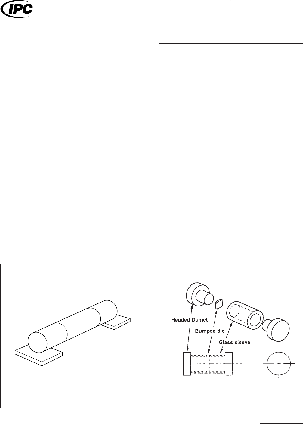
3.1 Basic Construction See Figures 1a and 1b.
3.1.1 Termination Materials End terminations should be
solder-coated with a tin/lead alloy. The solder should contain
between 58 to 68% tin. Solder may be applied to the termi-
nation by hot dipping or by plating from solution. Plated sol-
der terminations should be subjected to post-plating reflow
operation to fuse the solder. The tin/lead finish should be at
least 0.0075 mm [0.0003 in] thick. The terminations should be
symmetrical, and should not have nodules, lumps, protru-
sions, etc., that compromise the symmetry or dimensional tol-
erances of the part.
The most common termination materials include palladium-
silver alloy, silver, and gold. Solder finish applied over precious
metal electrodes should have a diffusion barrier layer between
the electrode metallization and the solder finish. The barrier
layer should be nickel or an equivalent diffusion barrier, and
should be at least 0.00125 mm [0.00005 in] thick. The end
termination shall cover the ends of the components, and shall
extend around the entire periphery.
3.1.2 Marking Parts are available with or without marked
values.
3.1.3 Carrier Package Format Bulk rods, 8 mm tape/4
mm pitch is preferred for best handling. Tape and reel speci-
fications provide additional requirements.
3.1.4 Resistance to Soldering Parts should be capable of
withstanding five cycles through a standard reflow system
operating at 215°C. Each cycle shall consist of 60 seconds
exposure at 215°C. Parts must also be capable of withstand-
ing a minimum of 10 seconds immersion in molten solder at
260°C.
IPC-782-8-5-1a
Figure 1a Metal electrode face component construction
IPC-782-8-5-1b
Figure 1b Break-away diagram of MELF components
IPC-SM-782
Surface Mount Design
and Land Pattern Standard
Date
5/96
Section
8.5
Revision
A
Subject
Metal Electrode Face
(MELF) Components
Page1of4
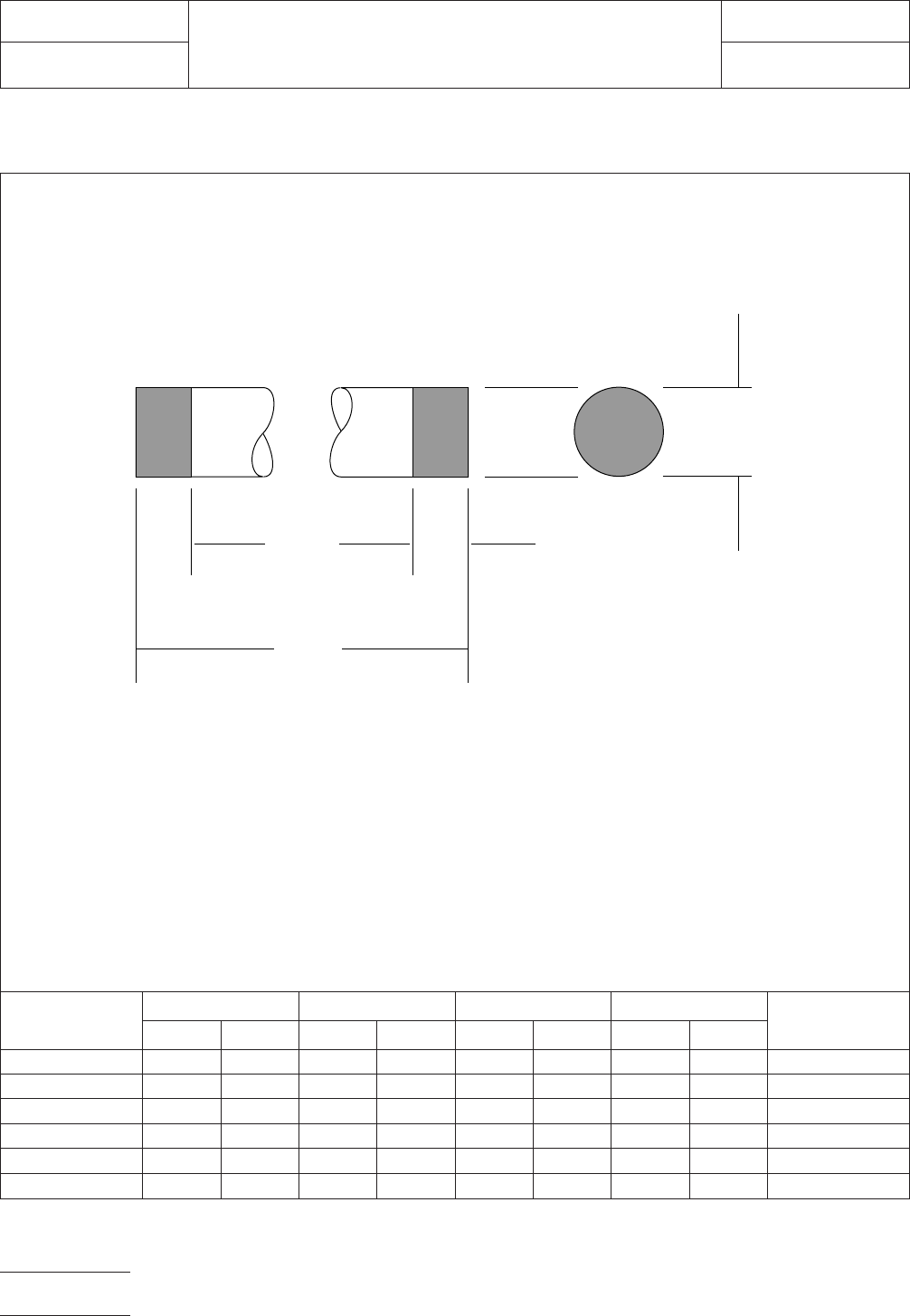
4.0 COMPONENT DIMENSIONS
Figure 2 provides the component dimensions for metal electrode face components (MELFs).
Component
Identifier (mm)
[in]
L (mm) S (mm) W (mm) T (mm)
Component Typemin max min max min max min max
SOD-80/MLL 34 3.30 3.70 2.20 2.65 1.60 1.70 0.41 0.55 Diode
SOD-87/MLL 41 4.80 5.20 3.80 4.25 2.44 2.54 0.36 0.50 Diode
2012 [0805] 1.90 2.10 1.16 1.44 1.35 1.45 0.23 0.37 0.10 mW resistor
3216 [1206] 3.00 3.40 1.86 2.31 1.75 1.85 0.43 0.57 0.25 mW resistor
3516 [1406] 3.30 3.70 2.16 2.61 1.55 1.65 0.43 0.57 0.12 W resistor
5923 [2309] 5.70 6.10 4.36 4.81 2.40 2.50 0.53 0.67 0.25 W resistor
Figure 2 Metal electrode face component dimensions
W (DIA.)
S
L
T
▼
▼
▼
▼
▼
▼
▼
IPC-782-8-5-2
IPC-SM-782
Subject
Metal Electrode Face (MELF) Components
Date
5/96
Section
8.5
Revision
A
Page2of4
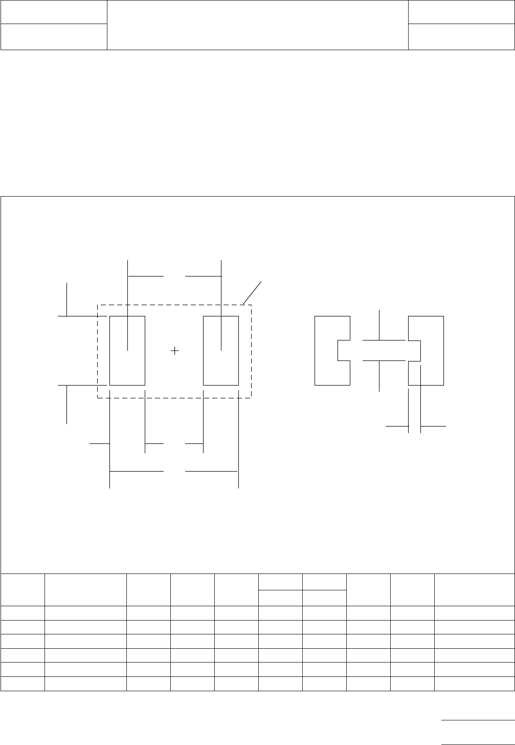
5.0 LAND PATTERN DIMENSIONS
Figure 3 provides the land pattern dimensions for metal elec-
trode face components (MELFs). These numbers represent
industry consensus on the best dimensions based on empiri-
cal knowledge of fabricated land patterns.
In the table, the dimensions shown are at maximum material
condition (MMC). The least material condition (LMC) should
not exceed the fabrication (F) allowance shown on page 4.
The LMC and the MMC provide the limits for each dimension.
The dotted line in Figure 3 shows the grid placement court-
yard which is the area required to place land patterns and
their respective components in adjacent proximity without
interference or shorting. Numbers in the table represent the
number of grid elements (each element is 0.5 by 0.5 mm) in
accordance with the international grid detailed in IEC publica-
tion 97.
RLP No.
Component
Identifier (mm) [in] Z (mm) G (mm) X (mm)
Y (mm) C (mm)
AB
Placement Grid
(No. of Grid
Elements)ref ref
200A SOD-80/MLL-34 4.80 2.00 1.80 1.40 3.40 0.50 0.50 6x12
201A SOD-87/MLL-41 6.30 3.40 2.60 1.45 4.85 0.50 0.50 6x14
202A 2012 [0805] 3.20 0.60 1.60 1.30 1.90 0.50 0.35 4x8
203A 3216 [1206] 4.40 1.20 2.00 1.60 2.80 0.50 0.55 6x10
204A 3516 [1406] 4.80 2.00 1.80 1.40 3.40 0.50 0.55 6x12
205A 5923 [2309] 7.20 4.20 2.60 1.50 5.70 0.50 0.65 6x18
Figure 3 Metal electrode face component land pattern dimensions
▼
▼
▼
▼
▼
▼
▼
▼
▼
C
G
Z
X
Y
▼
▼
▼
▼
A
Optional detent pattern
B
▼
Grid placement
courtyard
IPC-782-8-5-3
IPC-SM-782
Subject
Metal Electrode Face (MELF) Components
Date
5/96
Section
8.5
Revision
A
Page3of4