N7201A616E00_0317.pdf - 第278页
NPM-W 2 EJM7DE-MB-04 O-00 4-1-3 -1 Inspection specifica tions Operating procedure 4-1-3 ■ Component Camera resolution of 18 μ m (type A): 0603 chip or larger, QFP with the lead pitch of 0.4mm or more Camera resolution of…
NPM-W2 EJM7DE-MB-04O-00
4-1-2-2
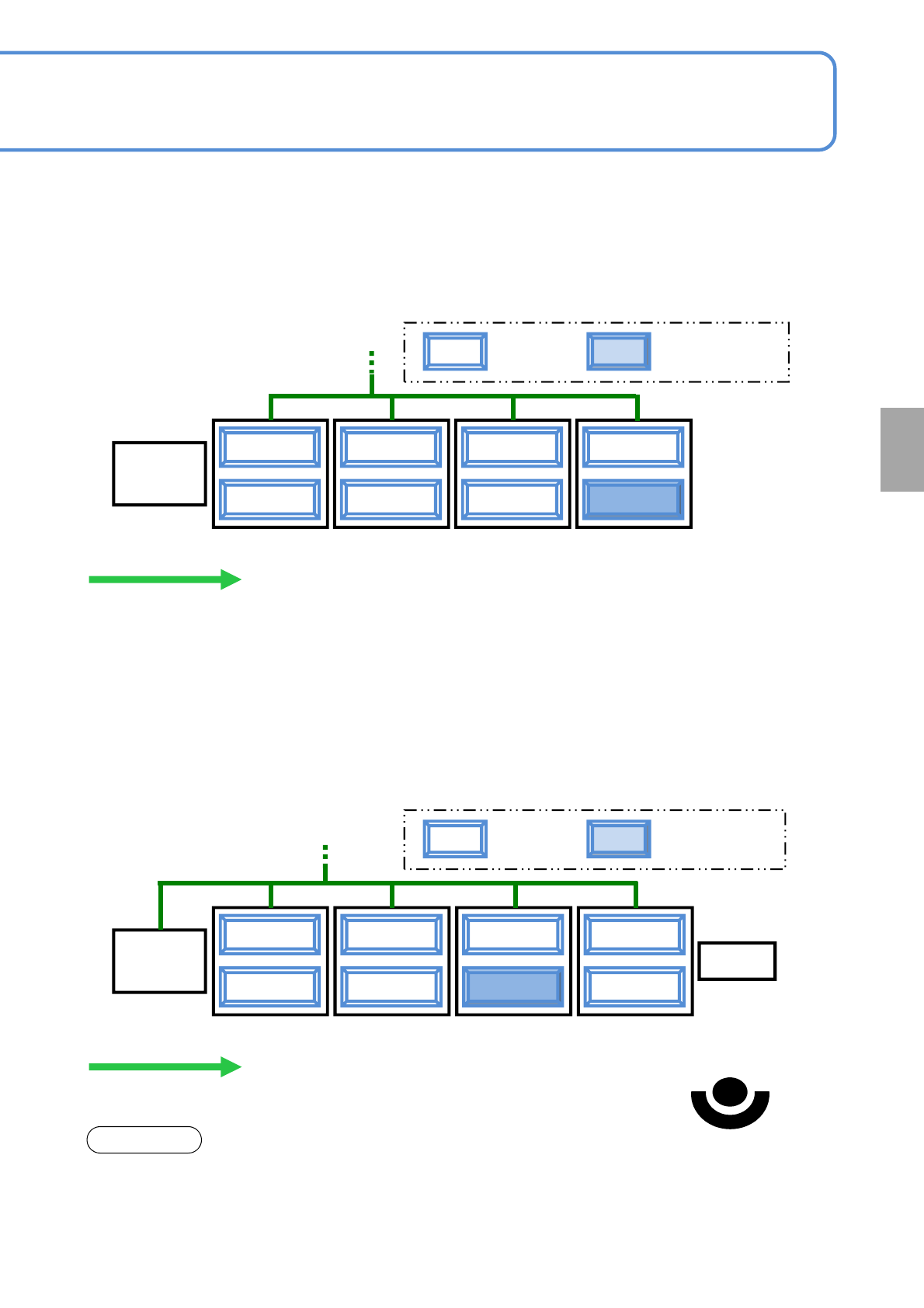
■Type 2
Mainly for the purpose of making the length of production line shorter, any ejection conveyor that performs
reload operation or reworks PCBs will not be placed in the line.
●In the case where the machine equipped with an inspection head for solder inspection use is placed first in
the production line (→P.5-1-2)
NPM-W2
Screen
printer
NPM-W2
(PCB flow)
Placement
head
Inspection head
(component
inspection)
NPM-W2 NPM-W2
■Type 3
The machine equipped with the inspection head (component inspection) will be placed last but one in the
production line (the second machine from the last one).
●Components that need to be checked for foreign bodies shall be placed as follows, provided that the
components include both reel and tray types.
However, you cannot conduct post-placement component inspection or reload operation in downstream
processes after a component is placed.
●In the case where the machine equipped with an inspection head for solder inspection use is placed first in
the production line (→P.5-1-2)
NOTICE
Reel
NPM-W2
Screen
printer
NPM-W2
Ejection conveyor
(PCB flow)
Placement
head
Inspection head
(component
inspection)
NPM-W2
Tray
NPM-W2
(Removal/rework of PCB)
●To rework or remove a PCB using the ejection conveyor, it is necessary to set up the position of the
ejection conveyor placed in the line with LNB. Please use “LNB configuration information” of LNB for setting
“Ejection conveyor” to the position of the ejection conveyor in the line.
For information on how to set up, (→ Chapter 4 in [LNB] operating instruction)
Component
inspection
NPM-W2 EJM7DE-MB-04O-00
4-1-3-1
Inspection
specifications
Operating procedure
4-1-3
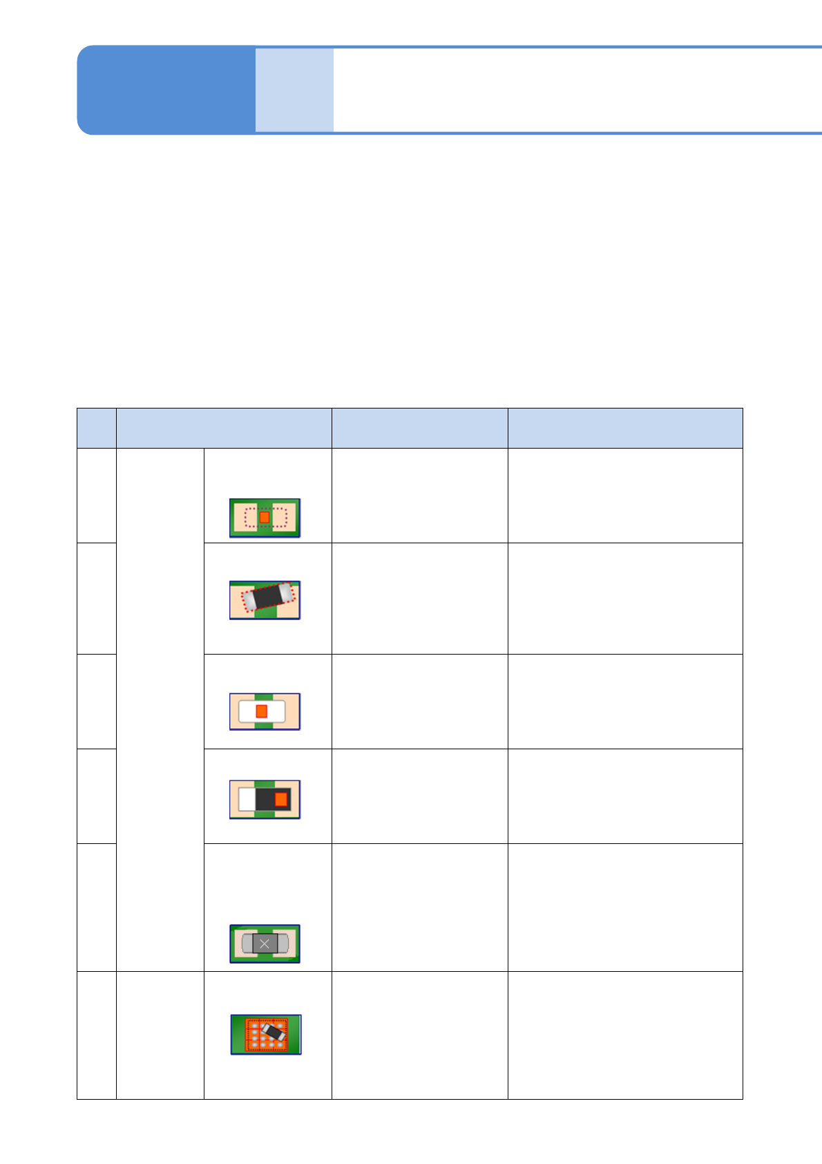
■Component
Camera resolution of 18μm (type A): 0603 chip or larger, QFP with the lead pitch of 0.4mm or more
Camera resolution of 9μm (type B): 0402chip or larger, QFP with the lead pitch 0.3mm or more
■Component size
Chip component: 10,000 points
■Number of available inspection points
■Inspection type
No.
Inspection type Inspection target Criterion
1
Post-
placement
inspection
Component
presence/absence
・There is no component
at the placement
position
・Judged as conforming if a PCB is
not displayed in color, or if a
component is displayed in color
2
Displacement ・The component
placement position is
shifted
・The component
placement angle is
shifted
・Judged as conforming if the shift
amount of the measured
electrode or component position
is within the set range
3
Flip over
*1)
・The placed component
is flipped.
・The placed component
is in a tombstoning
posture.
・Judged as nonconforming if the
reverse side or side of a
component is displayed in color
4
Wrong polarity
*2)
・The orientation of the
placed component is
incorrect
(for components with
olarity)
・Judged as conforming if a
component’s polarity is displayed
in color
5
Different
component
detection
(currently unused)
・The placed component
is different
・Judged as conforming if a
component is within the judgment
value in the template matching.
6
Pre-
placement
inspection
Foreign body
detection
・There is a dropped part
under the placement
component
(for components to be
placed by the
inspection-head-
installed machine)
・Judged as conforming if nothing
other than a PCB is displayed in
color
(excluding the already-placed
component area)
Over-
view
Square chip, SOP, QFP, BGA, CSP, aluminum electrolytic capacitor, volume, trimmer, coil, connector,
network resistance, transistor, diode, inductor, tantalum capacitor, cylinder chip

NPM-W2 EJM7DE-MB-04O-00
4-1-3-2
1)
For such a square chip resistor as has different colors on its front and back, the inspection for flip-over
can be set.
2)
The contrast of the polarity mark shall be clear. No dirt or blur. And also make sure that color or
brightness variability shall be narrow, and, as for IC, polar shape can be recognized by the image and
remains unchanged.
●The color and inspection area to be used for each inspection are set through the use of the pre-captured
image.
●For the PCB color, each color of PCB, solder, land, silk, and others is predetermined.
●For the placed component, if its color is missing by being shaded by its adjacent ones, the inspection
process may not be possible. And if there is no difference in color and brightness between PCB and
components, or if there are any variations in color and brightness due to the materials of PCB/components
or warp/deformation in PCB, the inspection process may not be possible. Also, please avoid installing the
machine in direct sunlight or near strong light.
Component
inspection