N7201A616E00_0317.pdf - 第325页
NPM-W 2 EJM7DE-MB-05O-0 0 ● To rework or remove a PCB using the ejection convey o r, it is necessary to set up the position of the ejection convey or placed in the line with LNB. Please us e “L NB configur ation informat…
NPM-W2 EJM7DE-MB-05O-00
Over-
view
System configuration
Operating procedure
5-1-2
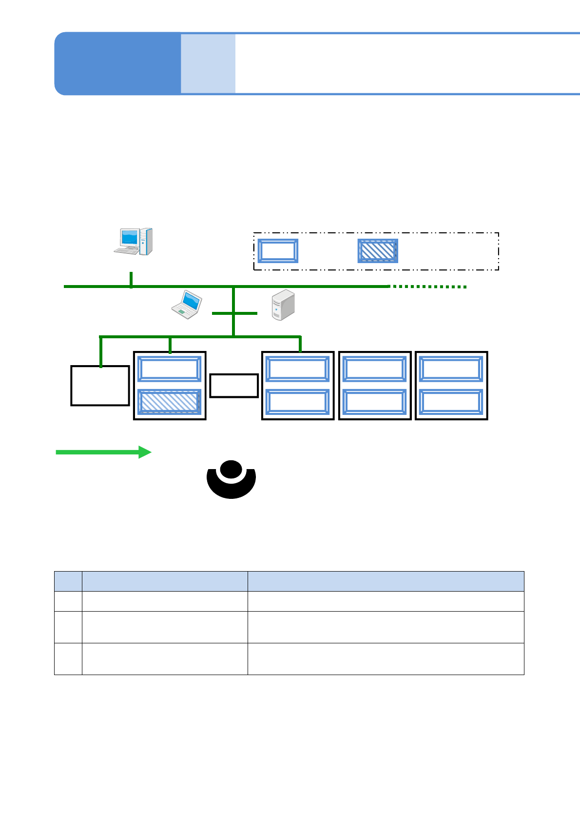
This section describes standard configuration of NPM-W2 system equipped with the inspection head
(solder inspection).
■Type 1
An ejection conveyor will be placed just downstream from the machine with the inspection head (solder
inspection) and, a conveyor, right between NPM-W2 and the ejection conveyor.
●Ejection conveyor: when a solder defect is found during inspection, it is used for locating the
defect/removing a defective PCB/repairing the PCB.
■Explanation of major peripheral devices (Phrases/words in this table will be used
in an abbreviated form in the rest of the manual)
No.
Name Explanation
1 DGS (Data Generation System) This creates and edits the production data.
2 LNB (Line Network Box)
The production information retrieved from NPM-W2 is saved.
(Inspection result information, etc.)
3 LWS (Line Work Station)
This edits and adjusts (tunes) the inspection data during
production.
1) For more information on the ejection conveyor specifications, please contact us.
5-1-2-1
NPM-W2
Screen
printer
NPM-W2
Inspection ejection
conveyor
コンベヤー
(Removal of PCB)
LWS LNB
(PCB flow)
DGS
Placement
head
Inspection head
(solder inspection)
NPM-W2 NPM-W2
1)
NPM-W2 EJM7DE-MB-05O-00
●To rework or remove a PCB using the ejection conveyor, it is necessary to set up the position of the
ejection conveyor placed in the line with LNB. Please use “LNB configuration information” of LNB for setting
“Ejection conveyor” to the position of the ejection conveyor in the line.
For information on how to set up, (→ Chapter 4 in [LNB] operating instruction)
NOTICE
5-1-2-2
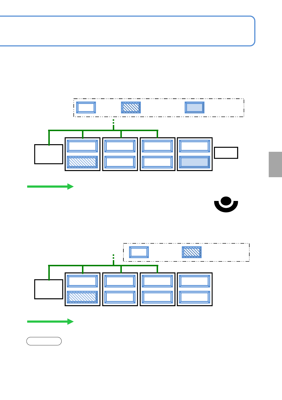
■Type 2
Mainly for the purpose of removing or repairing all defective PCBs at once after solder and component
inspections, an ejection conveyor will be placed at the end of the production line.
●When not placing components in the inspected defective solder paste on a per-PCB basis or on a per-NG
pattern basis (→P.5-5-2)
■Type 3
Mainly for the purpose of reducing time loss associated with operations including removal or repair of
defective PCBs, an ejection conveyor will not be placed.
●When not placing components in the inspected defective solder paste on a per-PCB basis or on a per-NG
pattern basis (→P.5-5-2)
NPM-W2
Screen
printer
NPM-W2
Inspection ejection
conveyor
(Removal/rework of PCB)
(PCB flow)
Inspection head
(Solder inspection)
Inspection head
(Component
inspection)
NPM-W2 NPM-W2
Placement
head
NPM-W2
Screen
printer
NPM-W2
(No removal/
repair of PCBs)
(PCB flow)
Placement
head
Inspection head
(Solder inspection)
NPM-W2 NPM-W2
Solder
inspection
NPM-W2 EJM7DE-MB-05O-00
Over-
view
5-1-3
Inspection
specifications
Operating procedure
5-1-3
Camera resolution 18 μm (Type A): Solder for chip component 100 x 150 μm or larger
Solder for package component φ150 μm or larger
Camera resolution 9 μm (Type B): Solder for chip component 80 x 120 μm or larger
Solder for package component φ120 μm or larger
■Target solder size
Component points: 10,000 points (the number of NPM-W2 placement data components)
Solder points: 30,000 points (the number of holes of mask hole data)
●Create the solder inspection data by converting and being tied the NPM-W2 production data to the
mask hole data (Gerber data)
■Number of available inspection points
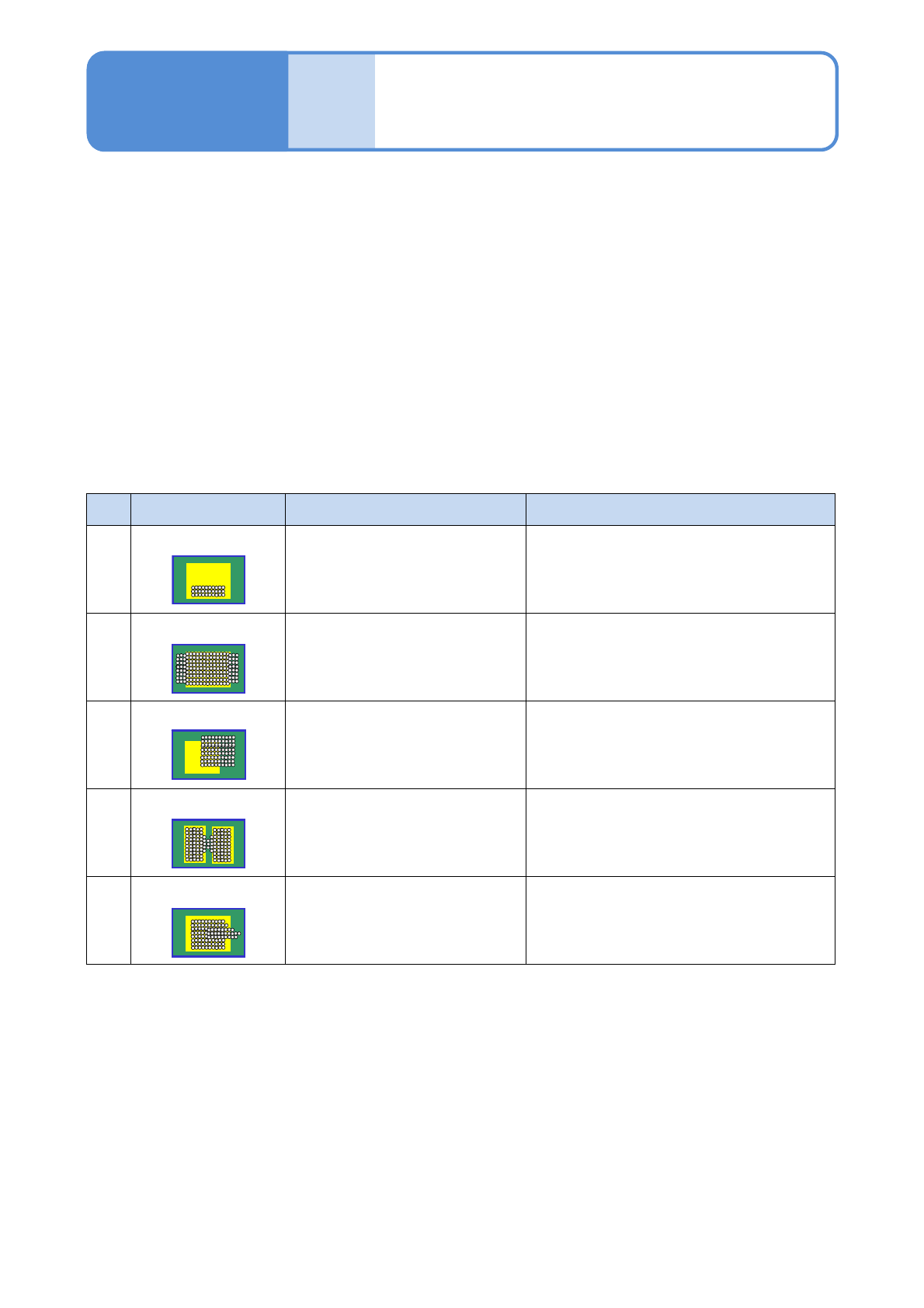
■Inspection type
No. Inspection type Inspection target Criteria
1
Fill
・Amount of solder is too short ・Judged as nonconforming if
measurement area ratio is less than
lower limit threshold
1)
.
2
Pervasion
・Amount of solder is too much ・Judged as nonconforming if
measurement area ration is exceed the
upper limit threshold.
3
Position
・Solder position is misaligned ・Judged as nonconforming if an amount
of measurement position misalignment
is exceeded the tolerance.
4
Bridge
・Bridged with adjacent solder ・Judged as nonconforming if the
measurement bridge width is exceeded
the tolerance bridge width.
5
Shape
・Bad solder shape ・Judged as nonconforming if the
measurement solder circumscribed
rectangle size is exceeded the tolerance.
The following items are inspected in comparison with the value measured for solder inspection based on
the hole area, the hole position (area center of gravity) and the hole size of the Gerber data for a mask
used for inspection data creation.
1) Defective solder: solder judged as nonconforming with the inspection head, or solder considered as
nonconforming by an operator.