N7201A616E00_0317.pdf - 第355页
NPM-W 2 EJM7DE-MB-05O-0 0 Dependin g on solder inspection conditions and the presence/a bsence of a defective PCB being at rest on the ejection co nveyor, the pro cessing method diffe rs. Use sol der in spection c onditi…
NPM-W2 EJM7DE-MB-05O-00
Defec-
tive PCB
process
5-5-1-1
Operating procedure
5-5-1
How to remove a defective PCB resulting in inspection and how to repair the defective PCB are explained.
3
1
Remove a
defective PCB
Restart
transportation
2
Repair the
defective part
● Turn ON a transport
restart switch (such as
the foot switch)
● The signal tower lights
up and a buzzer sounds.
●Cancel the [NG eject
reset] on the inspection
monitor.
(→P.5-4-3 ‘Explanation of
the screen’)
Overview
■Inspection ejection conveyor specifications
●PCB judged as defective suspends on the ejection conveyor and PCB judged as good does not suspend.
(→[NPM-W2 specification])
●When APC is used, do not insert the PCB except for the one being produced from the inspection ejection
conveyor.
●Process during transportation restart
A) If a PCB stays on the conveyor
The PCB is unloaded to the downstream process and the next PCB is allowed to load after unloaded.
B) If no PCB is on the conveyor after the PCB removed
PCB can be loaded from the upstream process.
NPM-W2 EJM7DE-MB-05O-00
Depending on solder inspection conditions and the presence/absence of a defective PCB being at rest on the
ejection conveyor, the processing method differs. Use solder inspection condition suitable for your production
pattern. (→P.5-5-2)
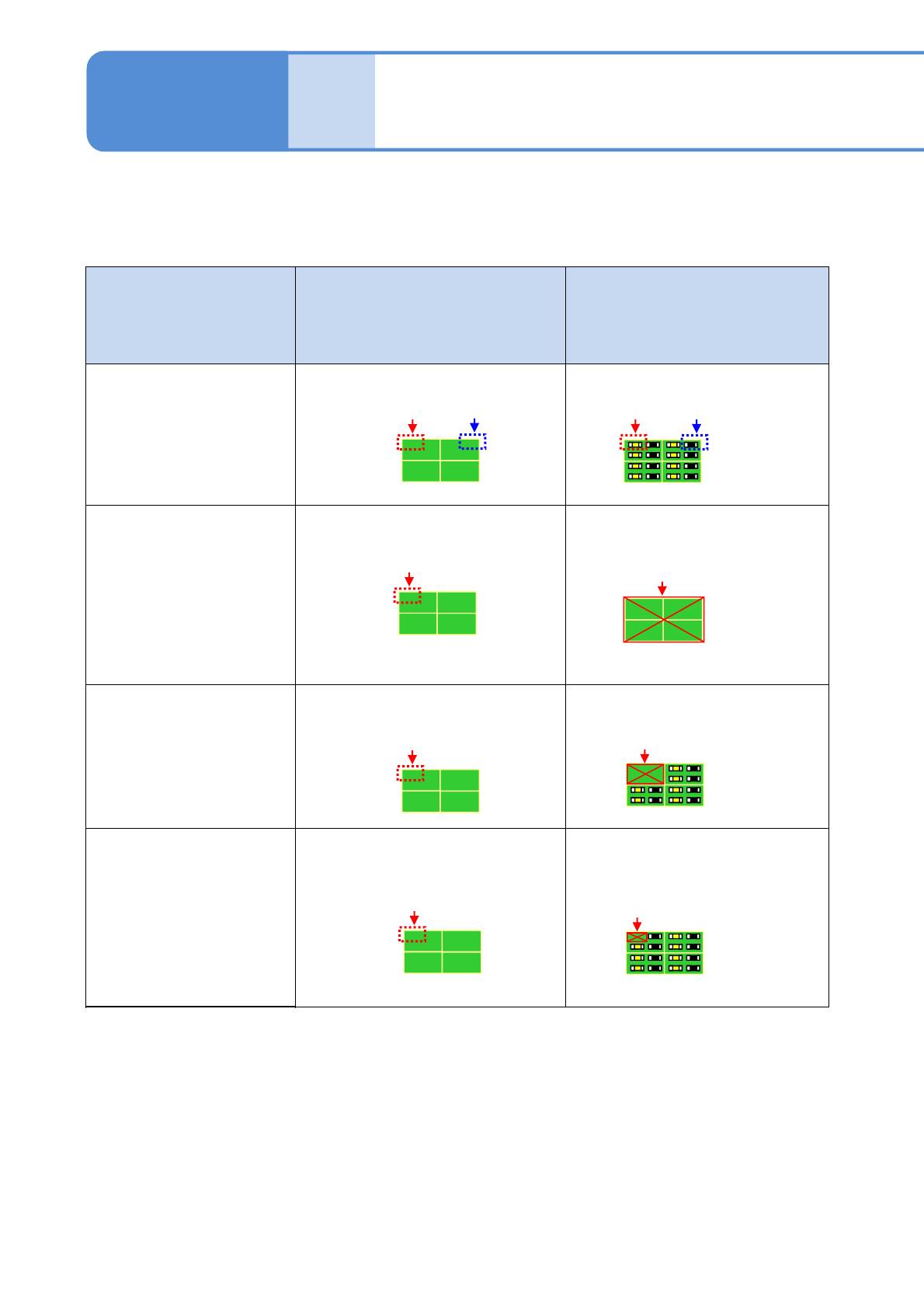
Solder inspection condition
Whether defective PCB
stops or not
1)
Processing method
Placement after all solders
inspection
Stops
●When skipping placement on PCB
3)
After removing an unplaced PCB,
dispose of it, or clean it for reuse.
●When selecting “NG placement”
Check or repair the defective part of
a component or solder.
Placement by pattern after all
solders inspection
No stopping
2)
●When skipping placement in a
pattern
3)
Dispose of a defective pattern with no
components placed.
●When selecting “NG placement”
Check or repair the defective part of a
component or solder.
Solder inspection right before
placement
Stops
●When skipping placement on PCB
4)
Check or repair the defective part of a
component or solder.
●When selecting “NG placement”
Check or repair the defective part of a
component or solder.
■Defective PCB processing
1) Since PCB cannot be repaired or removed before reflow without setting up an ejection conveyor, it is
recommended to use [Placement after all solder inspection] or [Placement by pattern after all solders
inspection] as the solder inspection condition.
2) When NG placement is selected for the defective part of solder during the over judge input, the ejection
conveyor stops for verification of PCB.
3) When component inspection comes after solder inspection, the component inspection will not be
conducted on the skipped pattern.
4) When component inspection comes after solder inspection, the component inspection will not be
conducted on the skipped PCB. Component inspection, however, will be conducted on the PCB flowing
into the process downstream from the ejection conveyor since it is considered as a repaired PCB.
5-5-1-2
Solder
inspection
NPM-W2 EJM7DE-MB-05O-00
Defec-
tive PCB
process
5-5-2-1
Processing method
Operating procedure
5-5-2
The processing method differs depending on the conditions and judgment result of solder inspection.
(→ Chapter 7 in [NPM-DGS] operating instruction)
●The judgment result is determined by the over judge input of solder inspection result. (→P.5-4-3)
Solder inspection condition Judgment result Processing method
Common to all conditions
For “OK” or “NG placement”
・Places components.
Placement after all solders
inspection
(After all solders are
inspected, placement only
for solder conforming
PCBs)
In the presence of more than one
“NG” solder on a PCB
・Skips placement on PCB.
Placement by pattern after
all solders inspection
(After all solders are
inspected, placement only
for solder conforming
patterns)
In the presence of more than one
“NG” solder in a pattern
・Skips placement in a “NG”
pattern.
Solder inspection right
before placement
(Inspection and placement
are alternatively carried
out and only conforming
components will be
placed)
In the presence of more than one
“NG” solder on a per-component
basis
・Skips placement of a component
corresponding to the “NG”
solder.
NG
placement
OK
NG
placement
OK
NG
NG
NG
Skip
Skip
Skip