N7201A616E00_0317.pdf - 第362页
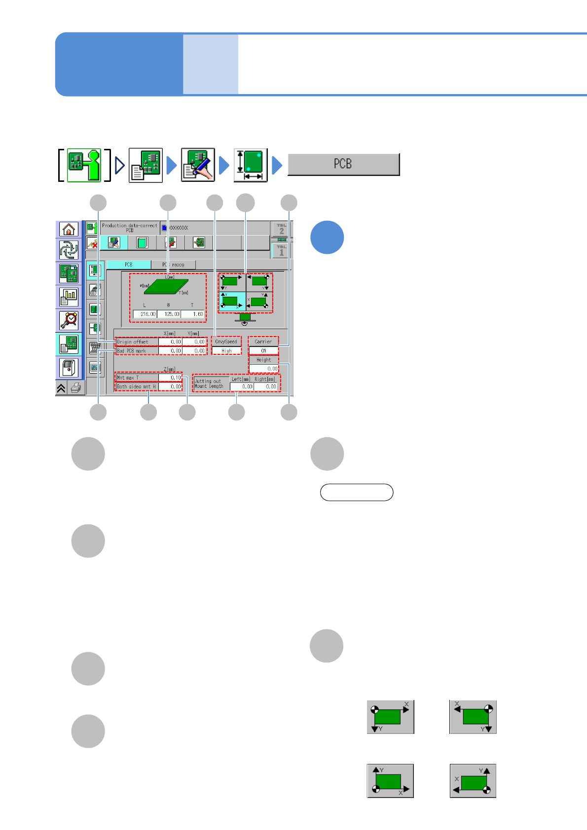
NPM-W 2 EJM7DE-MB-06O-0 0 Data editing 6-1-2 -1 A Origin offset D B C The maximum height of the components that are already placed on the front side. Both sides mnt H Bad PCB mark Edit the data by pointing the cursor to …

NPM-W2 EJM7DE-MB-06O-00
6-1-1-2
Setting
change
NPM-W2 EJM7DE-MB-06O-00
Data
editing
6-1-2-1
A
Origin offset
D
B
C
The maximum height of the components
that are already placed on the front side.
Both sides mnt H
Bad PCB mark
Edit the data by pointing the
cursor to the desired field
●Touching the screen opens the input
window.
Enter all the offset values of origin for
placement coordinates, PCB recognition
coordinates and bad mark coordinates.
Coordinates of bad mark.
●If the coordinates have this mark, it is
regarded as defective, where
placement will not be carried out.
●To edit it, set [ON] of [Detect Bad
Board Mark] of the soft switch.
(→P.6-1-20)
The maximum height of the components
that are already placed on the rear side.
Mnt max T
1
PCB data edit
Explains how to check and modify the PCB data.
E
PCB dimensions
Enter PCB dimensions.
Operating procedure
6-1-2
D C
A
B
G HE
J
F
I
●Right-front
reference
●Left-front
reference
●Right-rear
reference
●Left-rear
reference
F
Coordinate standard
Choose the PCB coordinate reference.
ATTENTION
Regarding PCB width, you may be able to
input a little bit larger value than the
maximum size of the machine PCB
specifications. It means that the
maximum width can be input on the
machine mechanism because we give
you extra space for variation of your PCB
size. However, regarding a PCB
exceeding the maximum size of PCB
specifications, we do not guarantee.
NPM-W2 EJM7DE-MB-06O-00
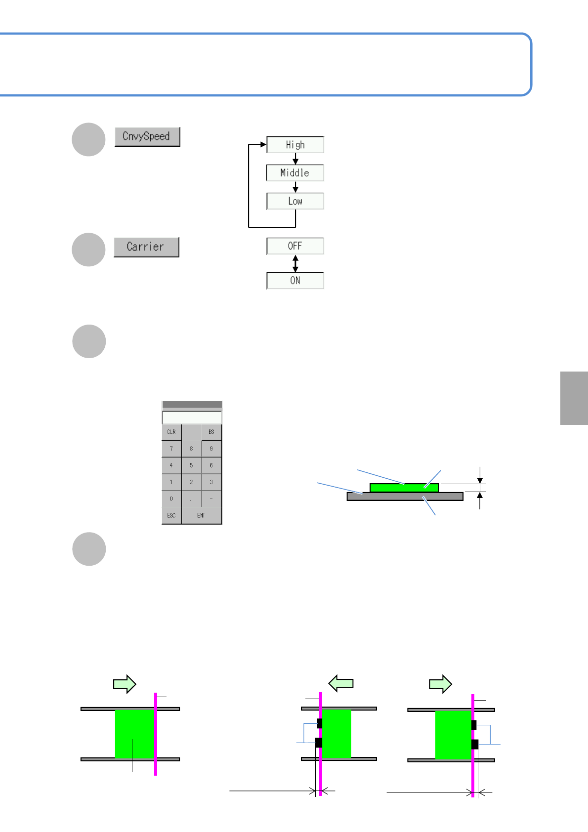
6-1-2-2
Choose whether to exist a carrier
PCB or not.
J
Jutting out Mount Length (Left, Right)
●If the placed component juts out from the PCB, the machine misjudges that the edge of the
placed component is the edge of the PCB, resulting in PCB recognition error.
So, entering the length of the jutting out placed component can carry out correct positioning.
■Normal PCB positioning
■Placed component jutting out of PCB edges
PCB
Reference
Placed
components
Reference
●Enter max. length in cases where components already placed juts out of right or left PCB edges.
Input range : 0 to 9 mm
Length of a placed
component jutting out (left)
G
Choose a PCB transfer
speed.
H
PCB flow direction
Placed
components
Reference
Length of a placed
component jutting out (Right)
PCB flow direction PCB flow direction
I
Touching the numerical part on the
screen opens the input window (See
below).
■When ’Yes’ selected
Height
●Enter the difference in height between a placement
surface and a clamp surface of the carrier PCB
when the carrier PCB is used. If the placement
surface is higher than the clamp surface, enter the
positive value, is it is lower, enter the negative
value.
Placement surface
Clamp surface
PCB
Carrier PCB
Height
●Height input (for positive value)
Setting
change