N7201A616E00_0317.pdf - 第638页
NPM-W 2 EJM7DJ-MB-08O-00 Over- view Operating procedure 8-1-1 8-1-1 -1 ● Eac h target machine is req uired for optional settings befor e use of APC sys tem . ● Items ind icated with are a standard fea ture in s older ins…

8 APC System
(option)
NPM-W2 EJM7DJ-MB-08O-00
Over-
view
Operating procedure
8-1-1
8-1-1-1
● Each target machine is required for optional settings before use of APC system .
●Items indicated with are a standard feature in solder inspections. (No
APC license is required)
● When using each function, the production data setting is configured by DGS or LWS. (→[NPM-DGS 2D
inspection editor])
APC stands for Advanced Process Control system, a technology to control the processes using process data
obtained by constantly measuring each process for improvement of placement quality.
APC system in the NPM line performs the following controls so that it reduces placement defects caused by
printing position displacement from the land position.
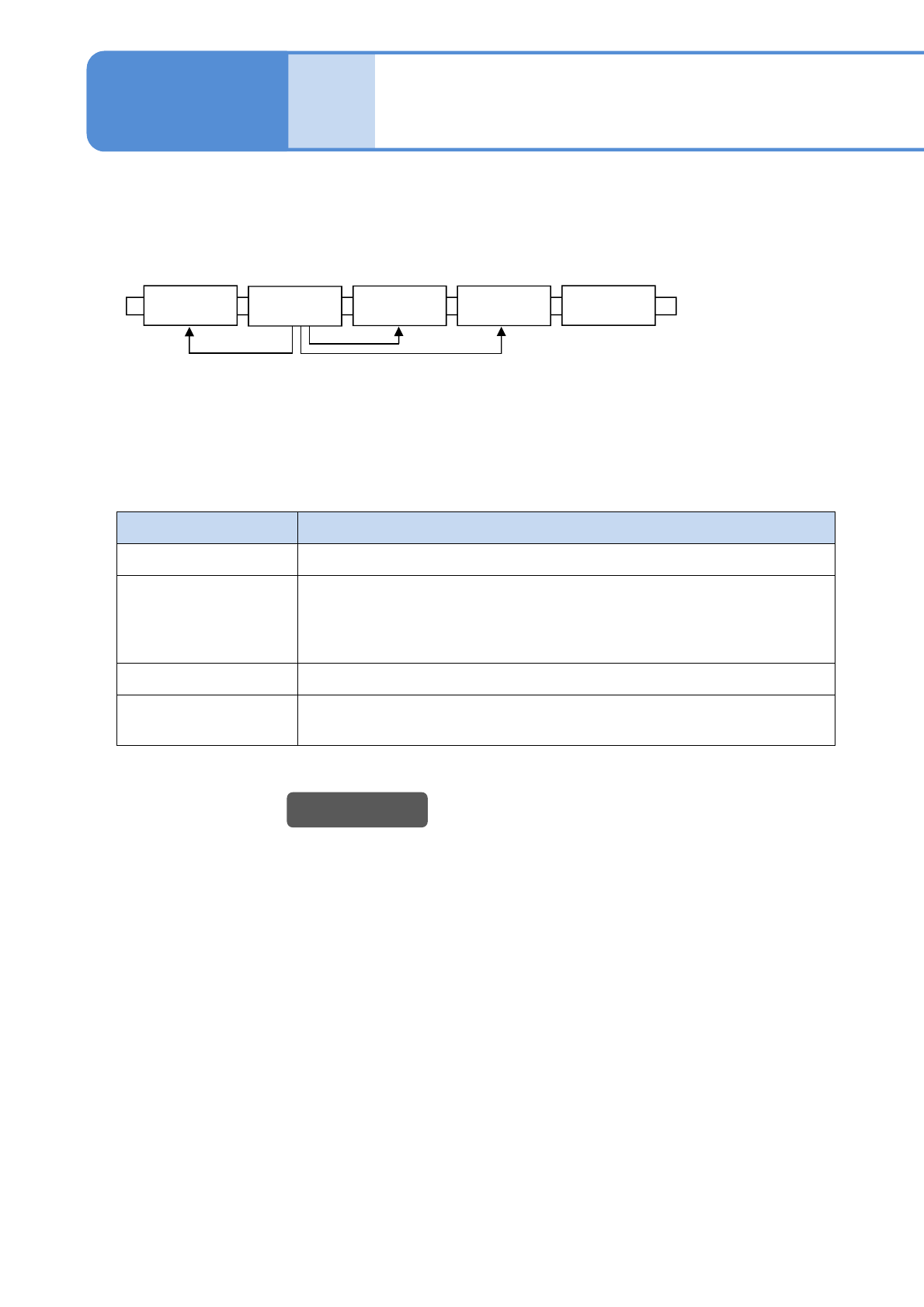
Solder inspection
standard
Solder
printing
Solder
inspection
Component
placement
Component
inspection
Reflow
①②③
・Feed-forward control to the downstream process
①Component placement: Components are placed onto the optimum and high accuracy position
based on the solder measurement position
②Component inspection: Components are inspected based on the corrected placement position
・Feedback control to the upstream process
③Solder printing: Solder paste is printed onto the optimum position based on the solder
measurement position
Function Applicable machines
Solder printing SPD, SP70, SPG
Solder inspection NPM inspection head: Inspection head installed on NPM (Installation to
NPM-TT is not supported)
Solder inspection machine manufactured by other companies: Please
contact us.
Component placement NPM placement head
Component inspection NPM inspection head: Inspection head installed on NPM (Installation to
NPM-TT is not supported)
Features 1
NPM-W2 EJM7DJ-MB-08O-00
8-1-1-2
APC
system
Desired effect
●Reduction in lifting, displacement or missing component defects of micro-component electrodes,
including 0402 and 0603
*1)
, leads to enhanced joint strength.
*1)
03015 is not applicable.
●Reduction in placement defects resulting from the price reduction of PCBs or the low land position
accuracy of carrier attachment/flexible PCB/ceramic PCB.
●Joint reliability improvement in ball components such as BGA and CSP, and reduction in void defects.
In case of any defect, components do not have to be placed in the downstream process so that waste
can be minimized.
●Reduction in chipping/cracking defects since the impact of component placement can be decreased.
■Placement quality improvement
●Defect patterns are specified based on the inspection results of printing solder paste or the lands (for
components to be transferred and placed) during production, which can cut down on the cost
associated with component losses.
●Land inspection before placement increases inspection reliability, and reduction in the costs associated
with preliminary inspections of PCBs and the defective pattern marking process.
●Pattern recognition time is reduced so that productivity and placement quality can be improved.
(High accuracy placement can be achieved based on PCB recognition criteria since the placement
position is controlled on a per-component basis in consequence of measurement of all solder positions
where components are placed.)
■ Cost reduction
We cannot assure that the above effects apply to the placement features of all our products.
NOTE
Solder inspection
standard
Solder inspection
standard