N7201A616E00_0317.pdf - 第646页
NPM-W 2 EJM7DJ-MB-08O-00 8-2-1 -1 System function details V arious functions 1 Operating procedure 8-2-1 Soldering position measurement function ■ Applicable component type Based on the coordinate orig in and the angle o…
NPM-W2 EJM7DJ-MB-08O-00
8-1-2-4
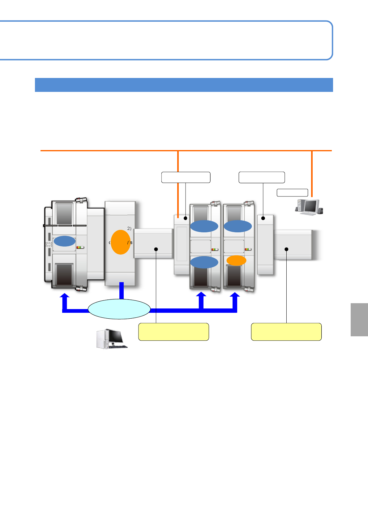
APC
system
System model chart (when a solder inspection machine manufactured by other company is used)
● As well as the license of the APC system, the license of interface software of the inspection machine
manufactured by other company is necessary per machine which receives the ACP correction data.
● NIP (PC used for converting the data of the inspection machine manufactured by other company) is
necessary.
● Please contact us about applicable models of an inspection machine manufactured by other company.
1) The following options are required.
FA computer, HUB unit, Power supply unit
2) Customer provides the conveyors.
Other
company’s
SPI
Other
company’s
SPI
2)
NPM-DGS
Conveyor L
1)
Ejection conveyor
2)
Ejection conveyor
2)
NIP
2)
APC correction data
PlacementPlacement
PlacementPlacement
PrintingPrinting
AOIAOI
PlacementPlacement
Conveyor R
NPM-W2 EJM7DJ-MB-08O-00
8-2-1-1
System
function
details
Various functions 1
Operating procedure
8-2-1
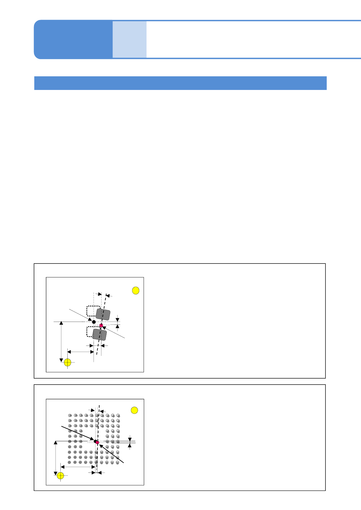
Soldering position measurement function
■Applicable component type
Based on the coordinate origin and the angle obtained by recognizing the PCB positioning mark, the
following soldering position misalignment amount is calculated on a per-placement component basis, and
the position is corrected relative to the logical placement coordinate.
■Calculating the misalignment amount of soldering positions
dθ:
The soldering position misalignment angle averages the difference, obtained relative to all solder, between
the theoretical angle and the measurement angle of the straight line connecting two positions of solder’s
center of gravity.
Dx, dy:
The soldering position misalignment amount averages the difference between the theoretical coordinate of
solder’s center of gravity relative to all solder and the measurement coordinate taking into account the
misalignment amounting equal to the above dθ.
The most relevant placement correction amount is calculated based on the soldering position
misalignment amount and the correction amount control parameters in response to each process, and
thus components are placed to the best suited position.
■Calculating the placement correction amount
Package component
①
⑨
③
④
⑦
⑧
⑤
⑥
②
① PCB positioning mark A
② PCB positioning mark B
③ Placement logical coordinate by positioning mark recognition
result
④ X logical coordinate of placement component
⑤ Y logical coordinate of placement component
⑥ Placement coordinate after correction
⑦ Printing misalignment amount dx of X direction
⑧ Printing misalignment amount dx of Y direction
⑨ Printing misalignment amount dx of θ direction
Square ship component
⑨
③
④
⑦
⑤
⑥
①
②
⑧
① PCB positioning mark A
② PCB positioning mark B
③ Placement logical coordinate by positioning mark recognition
result
④ X logical coordinate of placement component
⑤ Y logical coordinate of placement component
⑥ Placement coordinate after correction
⑦ Printing misalignment amount dx of X direction
⑧ Printing misalignment amount dx of Y direction
⑨ Printing misalignment amount dx of θ direction
There is no specific restriction. Specification for the solder to be measured is the same as the solder
inspection specification. See the operating instruction of the machine which performs solder inspection
(NPM inspection head or other company’s inspection machine).
1. Component placement feed forward
NPM-W2 EJM7DJ-MB-08O-00
8-2-1-2
APC
system
Based on coordinate origin and angle obtained from PCB positioning mark recognition, a position
misalignment amount and area difference from a logical value (mask gerber data of solder printing) is
calculated per mask aperture.
Dx, dy:
The difference between logical coordinates and measurement coordinates of the solder center of the
gravity is a solder position misalignment amount.
Area ratio:
Ratio [%] against the mask aperture area calculated from the gerber data is a solder area ratio.
A printing position to be corrected to the optimum solder printing position shall be the minimum
misalignment amount of solder position.
For details, see the operating instruction [NPM-DGS SP data editor] or the operating instruction of the
printer.
■Calculation of printing position correction amount
2. Solder printing feedback
① PCB positioning mark A
② PCB positioning mark B
③ Logical coordinates of the solder center of the gravity based
on the positioning mark recognition result
④ X logical coordinate of solder
⑤ Y logical coordinate of solder
⑥ Solder position misalignment amount dx in X-direction
⑦ Solder position misalignment amount dy in Y-direction
③
④
⑦
⑤
①
②
⑥
■Calculating a misalignment amount of soldering positions