N7201A616E00_0317.pdf - 第656页
NPM-W 2 EJM7DJ-MB-08O-00 System function details Pr ecautions on oper a tion 2 Operating procedure 8-2-3 8-2-3 -3 Case Solution If co mponent is not placed on land without APC correctio n Check placemen t coordinat e and…
NPM-W2 EJM7DJ-MB-08O-00
8-2-3-2
Location Large category Item Setting Remarks
Machine Special option
APC system
ON
License registration is required for all
sending and receiving machines.
DGS
1)
(Production
data)
Data creation job
editor
→
Communication
setting
(communication
switch)
Receiving inspection
information (APC)
ON
First machine: OFF
Middle machine: ON
Last machine: ON
Sending inspection
information (APC)
ON
First machine: ON
Middle machine: ON
Last machine: OFF
2D inspection
editor
→
PCB detailed
data setting
FF placement
control
ON For placement position correction
FF inspection
control
ON
For component inspection position
correction
Inspection NG skip
ON
For placement skip by the inspection
result
2D inspection
editor
→
Component
detailed setting
FF placement
control
ON For placement position correction
FF placement
control direction
(X direction)
ON For X direction position correction
FF placement
control direction (Y
direction)
ON For Y direction position correction
FF placement
control direction
(rotation direction)
ON
With angle correction
(Package component, connector, etc.)
OFF
With or without angle correction
(Chip components)
Specifying
measurement
target component
for FF correction
ON
APC mode: [APC correction per
pattern]
●Set more than one point per pattern.
APC mode: [Two points APC
correction]
●Set more than two points per
pattern.
OFF
APC mode: [ACF correction per
mount]
●The setting is not required.
Soft switch Inspection ON Solder inspection is required
■Required setting items
1)How to setup, (→Chapter 2 ‘EDITING THE PRODUCTION DATA’
in the [NPM-DGS 2D inspection editor] Operating Instruction)
Solder inspection
standard
APC
system
NPM-W2 EJM7DJ-MB-08O-00
System
function
details
Precautions on
operation 2
Operating procedure
8-2-3
8-2-3-3
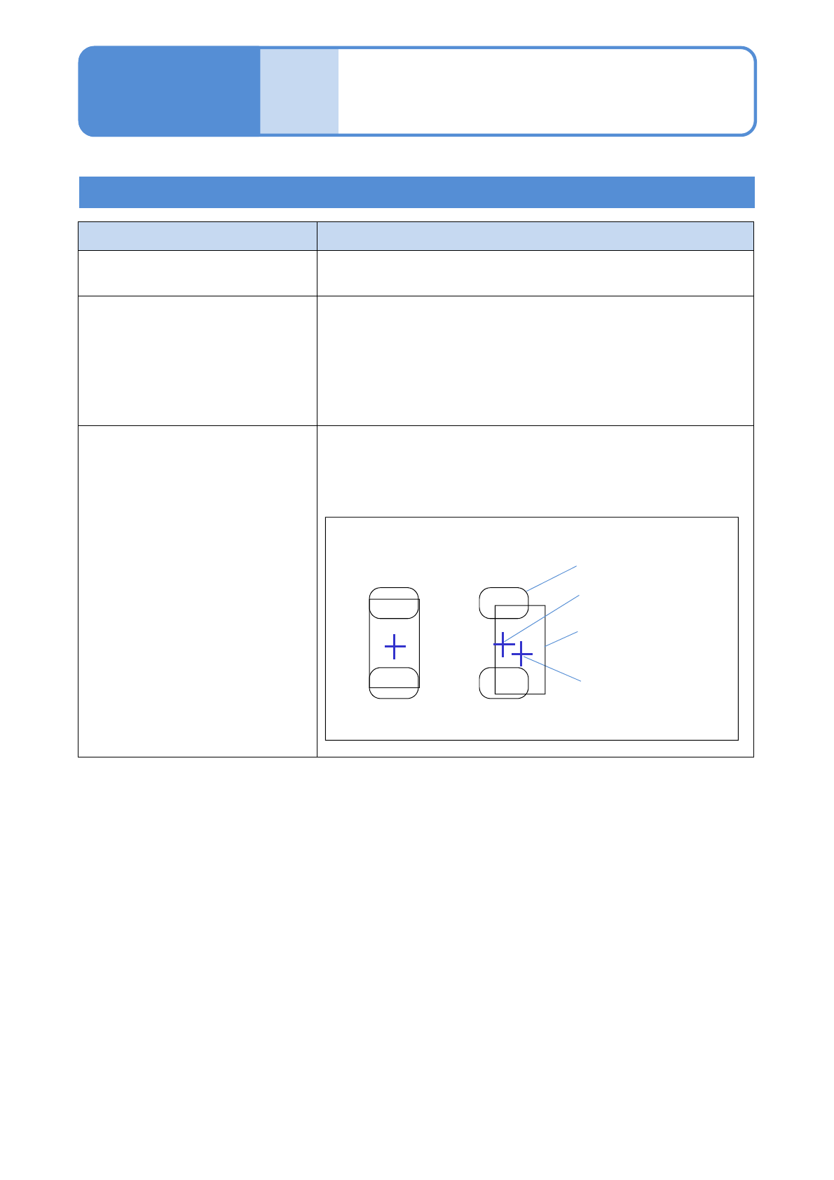
Case Solution
If component is not placed on land
without APC correction
Check placement coordinate and parameters.
Specified component has a certain
amount of misalignment
Check if coordinates and relative positions of the placement
coordinate data and the gerber data for mask solder printing are
correct, and also check that the data is matched to the data actually
used for production.
●When both data sets are merged by DGS, the relative relation
between the placement coordinate and solder position is recorded,
and the correction position is calculated based on that data.
If a flat offset is applied to all PCBs
Check if the PCB recognition coordinate is correct. Also, check that
the relative position is correctly matched (the center coordinate of
two solder centers for a chip component should be matched to the
placement coordinate of the component) when the placement
coordinate data and the gerber data are merged by DGS.
Margining placement coordinate data and gerber data
Mask hole data
Relative
position OK
Relative
position NG
Mask hole center
Component
placement coordinate
Component outer
data
If a placement position is misaligned before reflow
1)
1) The design value shall be used for the placement coordinate data and PCB recognition coordinate data.
After data creation, if the data of the placement coordinate is edited based on the actual component, APC
correction may not perform properly.
The production method by using the APC system corrects the data to produce conforming PCBs with
considering influence on solder misalignment caused by PCB and mask deformation, and other factors.
Because component variation is correctly measured, the design value must be used for the placement
coordinate data and the PCB recognition coordinate data.

9 At a Glance