N7201A616E00_0317.pdf - 第699页
NPM-W 2 EJM7DE-MB-09O -00 9-1-8 -2 For the purpose of preventing the defe ct PCB from mounting, the PCB warpage (heigh t) is measured. PCB warpage correction function *1) At a glance Appearance The same sensor of the loc…
NPM-W2 EJM7DE-MB-09O-00
9-1-8-1
Appearance
PCB
Thickness 0.3 to 8.0 mm
Material Glass epoxy, Paper Phenolic (Ceramic: custom support)
Measured
surface
material
The area of 1.5 x 1.5 mm or larger on the copper foil + the resist surface,
the copper foil surface, the silk surface or the ceramic surface.
Transparent and translucent area are excluded. (e.g. the surface of glass
epoxy composite material)
Function
Local PCB
height control
function
The PCB height (warpage) adjacent to the drawing position is
measured at multiple points in order to correct and optimize the
drawing height.
PCB warpage
acceptable
value
detection
function
If the difference equal to the measurement results of multiple
points exceeds the acceptable value, the occurrence of
defects in quality is prevented by detecting the error before
drawing.
Measure
ment
condition
Height
PCB upper surface ±4 mm
Area
The measurement point needs to be placed and set 5 mm
inside the edge of the PCB.
Measurement time
0.5 s (30 x 30 mm in an optimal condition, with 4-point measurement)
For the purpose of enhancing the drawing quality, the PCB warpage (height) is measured.
∗ Install to the X-axis mounted with the dispensing head.
∗ Measurement information is not communicated between machines.
∗ Only the dispensing height of the dispensing head can be corrected.
Local PCB height correction function
Specifi-
cation
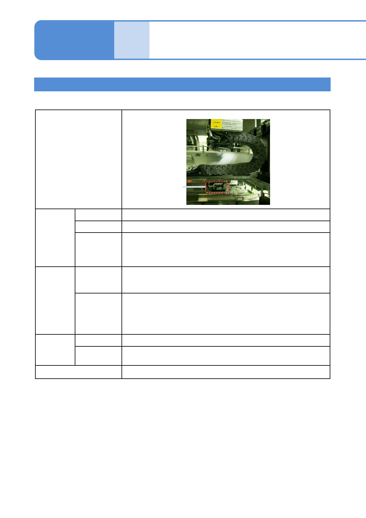
Height sensor 1
Operating procedure
9-1-8
Height sensor
NPM-W2 EJM7DE-MB-09O-00
9-1-8-2
For the purpose of preventing the defect PCB from mounting, the PCB warpage (height) is measured.
PCB warpage correction function
*1)
At
a glance
Appearance
The same sensor of the local PCB height correction function is used.
PCB
*2)
Thickness 1.6 to 8.0 mm
Material Glass epoxy
Measured
surface
material
There should be the area of 1.5 × 1.5 mm or larger on the copper foil +
the resist surface, the copper foil surface or the silk surface.
Transparent and translucent area are excluded. (e.g. the surface of glass
epoxy composite material)
PCB warpage
amount
Upper warp: 2 mm or less, lower warp: 2 mm or less, and warp
gradient:0.5 % or less, The difference in height of an edge line (transfer
direction): 1 mm or less.
Function
PCB warpage
acceptable
value
detection
If the measured result exceeds the tolerance, warning appears before
placement to prevent from quality defect. Tolerance warpage grade
(%) can also be checked.
Height control
Measures the PCB overall height (warpage) and controls the
placement height
Measured
data transfer
The data measured by the first machine in NPM-W2 is transferred to the
downstream machine.
The machine in downstream must be NPM-W2. Other than NPM-
W2(also including NPM-W), the data cannot be transferred.
Please ask us for the PCB which changes warpage shape every time
PCB clamps.
Measure
-ment
condition
Height
PCB top surface ±4 mm (Area to be measured. It is not PCB warpage
tolerance)
Area Area of 5mm from PCB edge and cutout.
Points
*3)
Overall warpage correction : 9 points or more (up to 25 points/PCB)
Pattern warpage correction : 9 points/pattern or more (up to 25
points/pattern)
Measurement time
3.0 s (750 × 510 mm in an optimal condition, with 9-point measurement)
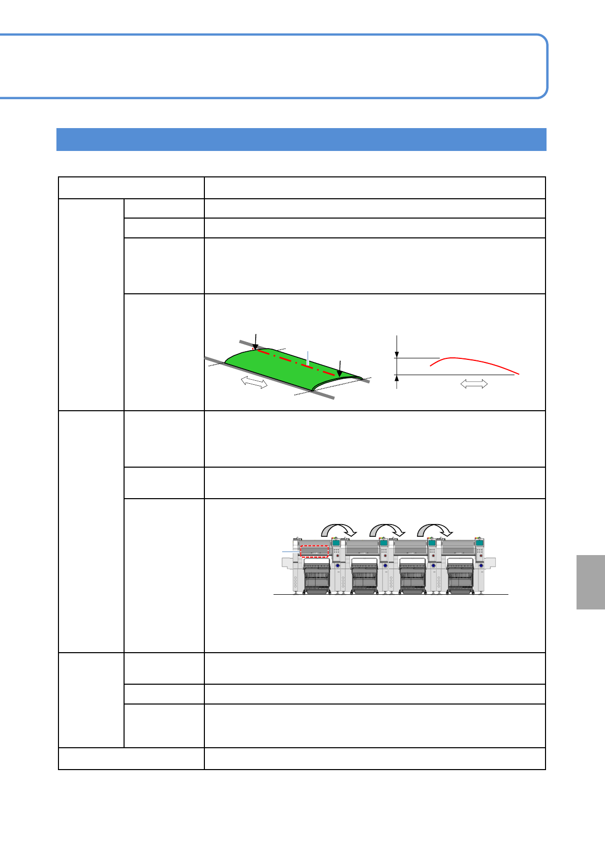
A
B
B
A
Edge line
Transfer direction
Transfer direction
1mmorless
Edge line
Height
sensor
NPM-W2 EJM7DE-MB-09O-00
9-1-8-3
*1) Installs to the machine in the combination of a placement head + a placement head.
PCB warpage measurement and data transfer can be carried out in the combination of a placement
head + a placement head, and the placement height is controlled by the stage with the placement head.
PCB warpage measurement on the machine with a placement head + a dispensing head, inspection
head or no head is not applicable.
The height sensor is installed to the front head for the single lane mode use. For dual lane mode, install
it to the front and rear heads.
*2) Correctable warpage by PCB warpage correction is the only PCB whose a cross section shape is a
U-shape simple curve.
For complex warpage, using pattern warpage correction allows correcting a PCB as simple curve
combinations.
As for a PCB with slip (cutout) or thin PCB, warpage shape may be complex, so that we recommend to
use pattern warpage correction. (→■Pattern warpage correction)
*3) For the maximum set number (total) of measuring points, see [9-1-1 Program data of machine
specifications].
Specifi-
cation
Operating procedure
9-1-8
Height sensor 2
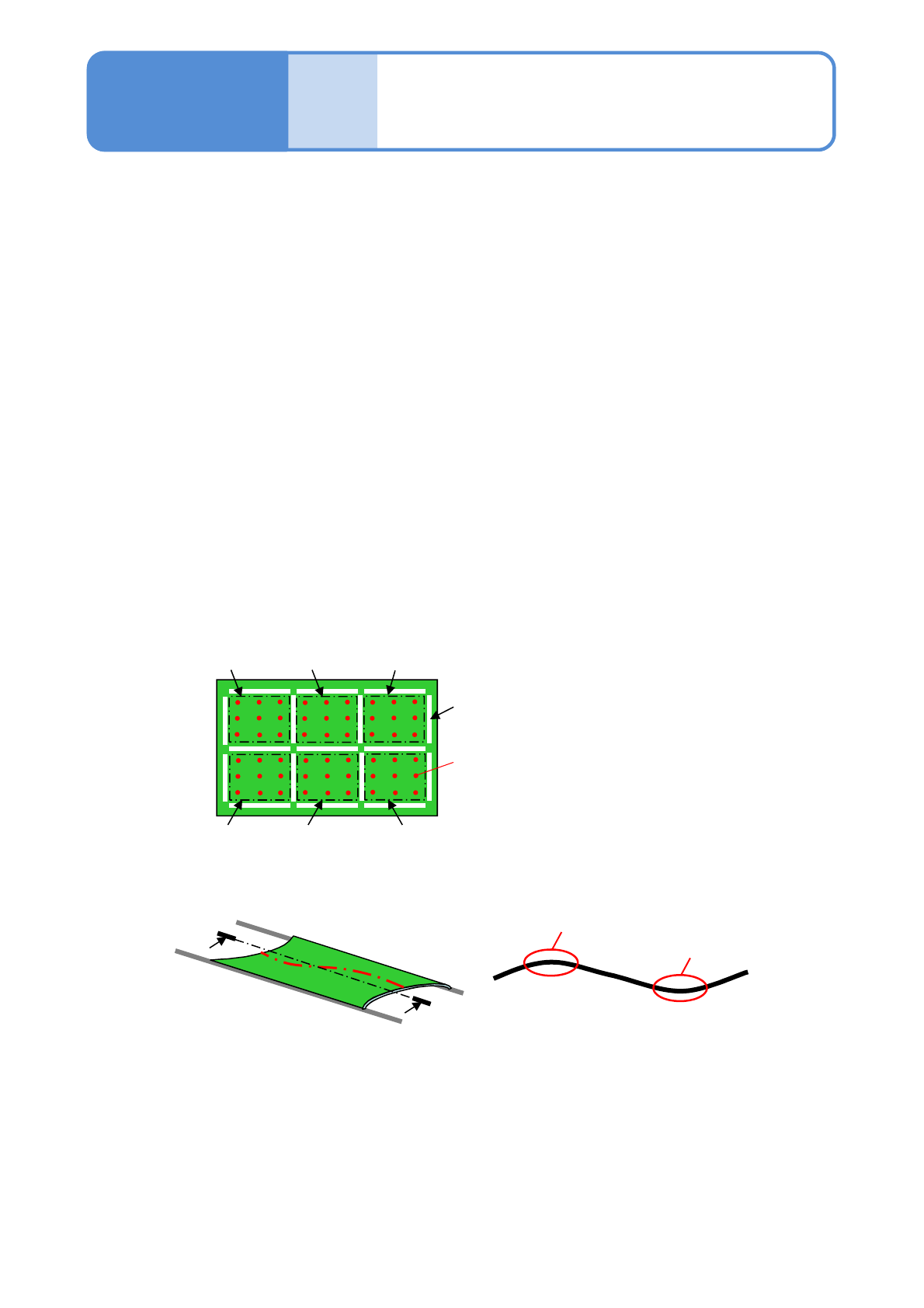
■Pattern warpage correction
Warpage correction at measuring point per pattern is called pattern warpage correction (see below).
As for a PCB with slip (cutout), warpage shape may be complex and not be smooth (uniformed) curve.
In such a PCB, we recommend to use pattern warpage correction.
Slit
Pattern1 Pattern2 Pattern3
Pattern4 Pattern5 Pattern6
Measurement
point
A
A
Upward warpage
Downward
warpage
A – A cross section
●Correction impossible warpage shape
Ex. ) Waving PCB