semi合集-English.pdf - 第117页
SEMI E15-0698 E2 © SEMI 1990, 2003 2 5.1.13 spacing — The minimum spacing between centroids (see Figure 2, S). 5.1.14 tool — Any piece of semiconductor fabrication or inspection equipm ent designed to proc ess wafers del…

SEMI E15-0698
E2
© SEMI 1990, 2003 1
SEMI E15-0698
E2
(Reapproved 0703)
SPECIFICATION FOR TOOL LOAD PORT
This standard was technically reapproved by the Global Physical Insterfaces & Carriers Committee and is the
direct responsibility of the North American Physical Interfaces & Carriers Committee. Current edition
approved by the North American Regional Standards Committee on March 12, 2003. Initially available at
www.semi.org May 2003; to be published July 2003. Originally published in 1990; previously published
March 2003.
E
This specification was editorially modified in November 2004 to correct an editorial error. Changes were
made to Table 1.
1 Purpose
1.1 This standard is intended to unify the interface
between process/inspection tools and automated wafer
carrier transport systems while maintaining
compatibility with human transport.
2 Scope
2.1 This specification deals with the mechanical
interface (load port) for wafer carrier transfer between
wafer carrier material transport systems, including
humans, and wafer fabrication/inspection equipment
(tools). The concept defines the placement and
orientation of a wafer carrier on a tool to allow
reasonable interfacing with mechanized material
movement systems without compromising human
access to perform the material exchange function.
NOTICE: This standard does not purport to address
safety issues, if any, associated with its use. It is the
responsibility of the users of this standard to establish
appropriate safety and health practices and determine
the applicability of regulatory or other limitations prior
to use.
3 Impact
3.1 Compliance with this specification requires the
placement of load ports on tools to specific heights,
orientations, and load depths. Restrictions are also
placed on clearances to obstructions which may be
adjacent to such ports.
4 Referenced Standards
4.1 SEMI Standards
SEMI E1 — Specification for 3 inch, 100 mm, 125
mm, and 150 mm Plastic and Metal Wafer Carriers
SEMI E19 — Standard Mechanical Interface (SMIF)
NOTICE: Unless otherwise indicated, all documents
cited shall be the latest published versions.
5 Terminology
5.1 Definitions
5.1.1 box — A protective portable carrier for a cassette
and/or substrate(s).
5.1.2 cassette — An open structure that holds one or
more substrates.
5.1.3 cassette centroid — A datum representing the
theoretical center of a stack of wafers in a cassette
formed by the pocket centerline and the “center” pocket
as defined by the location associated with dividing
dimension B3 by two (see SEMI E1, Figure 1).
5.1.4 cassette envelope — A rectangular volume with
vertical sides which completely contains a cassette,
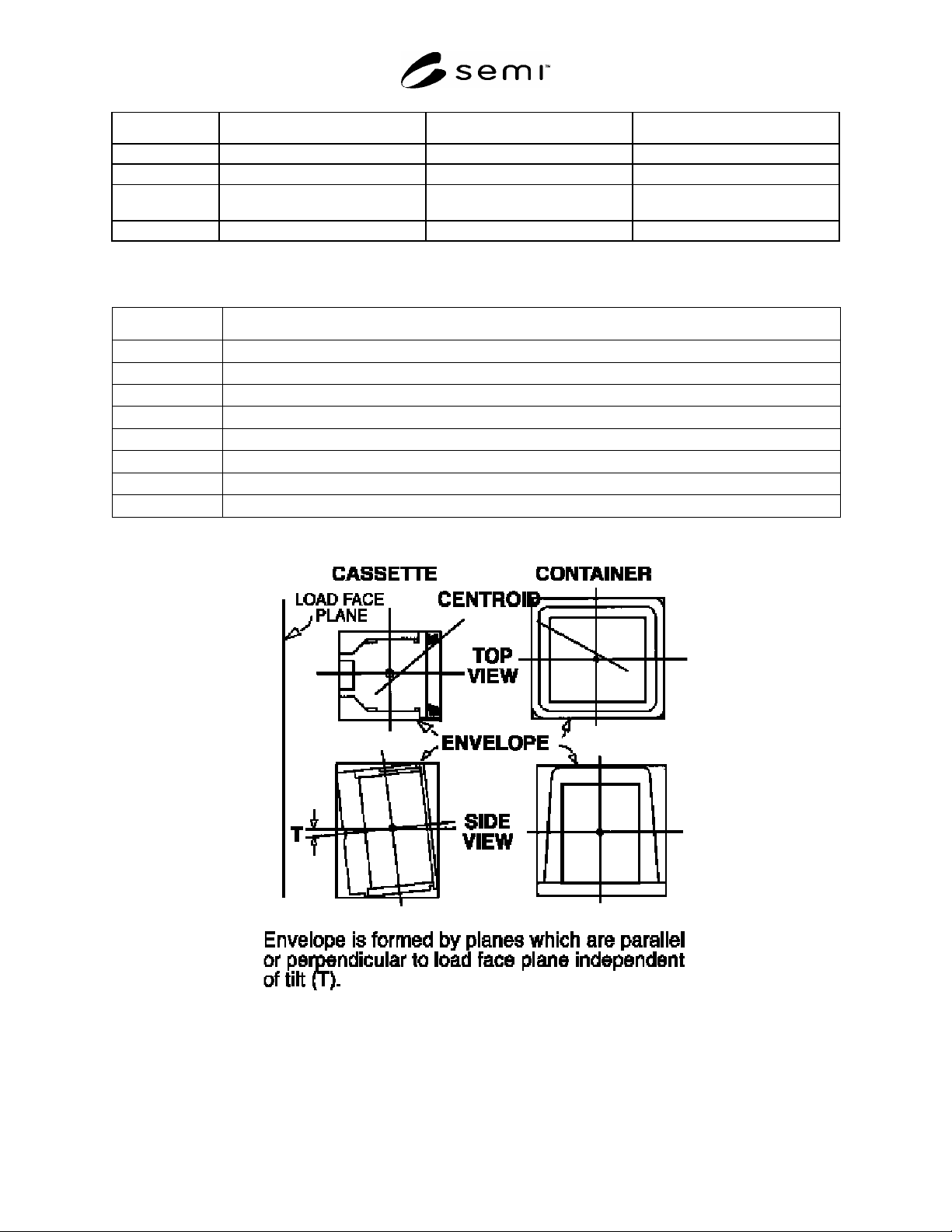
even if the cassette is tilted (see Figure 1).
5.1.5 enclosed load port — A load port with overhead
clearance obstructed by the tool.
5.1.6 global orientation — The general orientation of a
wafer carrier in a tool; may be vertical or horizontal.
5.1.7 load depth — The horizontal distance from the
load face plane to cassette centroid or carrier centroid
(see Figures 2 and 3 (D)).
5.1.8 load face plane — The furthest physical vertical
boundary plane from cassette centroid or carrier
centroid on the side (or sides) of the tool where loading
of the tool is intended (see Figures 2 and 3).
5.1.9
load height — The distance from the bottom of
the cassette or carrier to the floor at the load face plane
(see Figure 3 (H)).
5.1.10 load port — The interface location on a tool
where wafer carriers are delivered. It is possible that
wafers are not removed from, or inserted into, the
carrier at this location.
5.1.11 open load port — A load port with overhead
clearance unobstructed by the tool.
5.1.12 pod — A box having a Standard Mechanical
Interface (SMIF) per SEMI E19.
SEMI E15-0698
E2
© SEMI 1990, 2003 2
5.1.13 spacing — The minimum spacing between
centroids (see Figure 2, S).
5.1.14 tool — Any piece of semiconductor fabrication
or inspection equipment designed to process wafers
delivered in wafer carriers.
5.1.15 tilt — A small angle of offset from the normal
horizontal or vertical orientation of a cassette or wafer
carrier designed to preferentially align or keep wafers in
their intended place within the carrier/cassette (see
Figure 1, T).
5.1.16 wafer carrier — Any cassette, box, pod, or boat
that contains wafers.
5.1.17 wafer carrier centroid — A datum representing
the theoretical location of the center of a stack of wafers
in the carrier.
5.1.18 wafer carrier envelope — A rectangular volume
with vertical sides which completely contains a carrier,
even if the carrier is tilted (see Figure 1).
5.2 Description of Terms Specific to this Standard
5.2.1 carrier — Wafer carrier.
6 Ordering Information
6.1 The following items require communication
between the tool supplier and user and shall be included
in any request for quotation, quotation, or purchase
order:
6.1.1 If the tool has multiple load ports, provide the
spacing, S, between carrier centroids (see Section 7.8).
6.1.2 Specify what carrier (e.g., SEMI standard
cassette, pod) is to be accommodated by the load port.
6.1.3 Specify whether the load port is open or
enclosed.
6.1.4 Specify whether the wafer orientation is
horizontal (per Section 7.3.1) or vertical (per Section
7.3.2).
7 Requirements
7.1 The dimensions for the placement of a wafer
carrier on the load port of a tool are given in Table 1.
7.2 The standard is based upon the concept that any
wafer carrier can be used. Dimensions are usually
specified as clearances to wafer carrier envelopes (see
envelope concept in Figure 1).
7.3 The global orientation of the cassette or wafer
carrier is constrained to be parallel or perpendicular to
the load face plane. Allowable cassette orientations are:
7.3.1 For wafers horizontal, the opening of the cassette
must be opposite the load face plane, and the front
surface of the wafer must face up (see Figure 4);
7.3.2 For wafers vertical, the opening of the cassette
must face up, and the front surface of the wafer must
face the load face plane (see Figure 5).
7.3.3 This requirement also applies to cassettes in
pods.
7.4
The maximum tilt is 10 degrees.
7.5 The load height is specified as follows (see Figure
3):
7.5.1 Dimension H is 900 mm (~35.4 in.), fully
adjustable over ± 10 mm (~0.4 in.).
7.6 The maximum height above H of an obstruction
between the load face plane and the carrier envelope
(such as for an alignment device or identification tag
reader) is 50 mm (~2 in.) (see Dimension H1 in Figure
3).
7.7 Clearances (C1, C2, and C3) are defined with
respect to the largest carrier envelope required. For
cassettes, envelopes are defined using cassette
dimensions from SEMI E1. For pods or other wafer
carriers, envelopes are defined using the carrier
standard (if any) or the carrier manufacturer's
specifications (see Figure 1 for concept and Figures 2
and 3 for use).
7.8 Dimension S specifies the recommended minimum
spacing between cassette/wafer carrier centroids. In any
case, if S violates clearance C1 in any application, then
C1 prevails (see Figure 2).
7.9 Tools with enclosed load ports shall have a
minimum vertical clearance, C3, above the cassette or
carrier at the load port. Open load ports shall have a
vertical clearance above the load port which is
unrestricted by the tool.
Table 1 Dimension Requirements, mm (inches)
Dimension Application Value, mm (in.) Notes
C1 minimum 75 (3)
C2 minimum 30 (1.2)
C3 minimum 225 (9) See Note 1
D maximum 250 (9.8)
SEMI E15-0698
E2
© SEMI 1990, 2003 3
Dimension Application Value, mm (in.) Notes
H range 900 (35.4) ± 10 (.4) See Note 2
H1 maximum 50 (2.0)
S 150 mm carriers
200 mm carriers
350 (13.8)
400 (15.7)
See Section 7.8.
T maximum 10 degrees
NOTE 1: Applies to tools with enclosed port; otherwise, clearance above the port must be unrestricted by the tool (see Section 5.8).
NOTE 2: Fully adjustable over ± 10 mm (~0.4 in.) range.
Table 2 Dimension Definitions
Dimension Description
C1 Minimum side clearance between one carrier envelope and another, or to vertical obstruction.
C2 Minimum rear clearance from carrier envelope to vertical obstruction.
C3 Minimum clearance above carrier envelope to horizontal obstruction on the tool.
D Maximum load depth to carrier centroid.
H Allowable load height to bottom of carrier envelope.
H1 Maximum height of horizontal obstruction above load height between load face plane and carrier envelope.
S Recommended minimum spacing between carrier centroids.
T Maximum cassette or wafer carrier tilt.
Figure 1
Envelope Concept