semi合集-English.pdf - 第170页
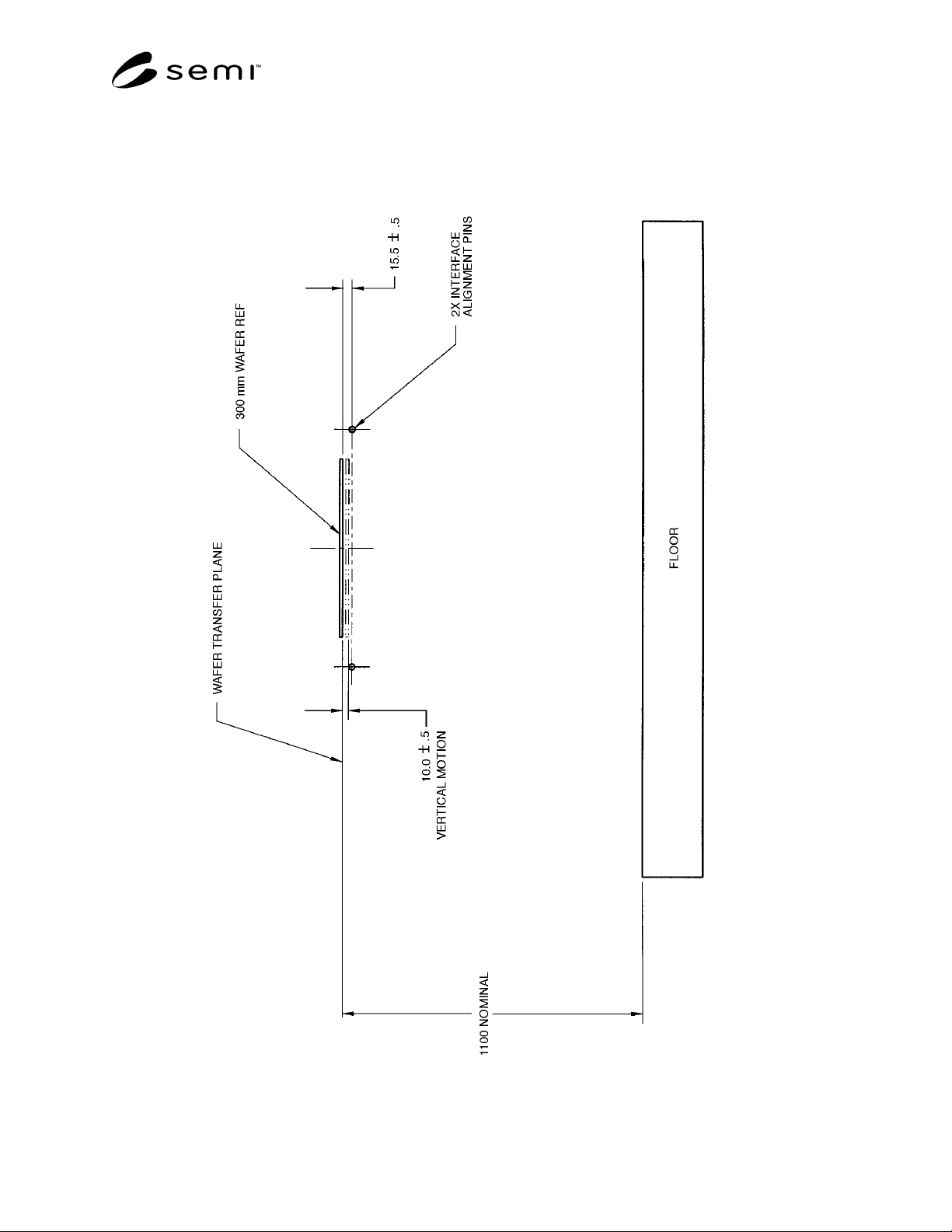
SEMI E21.1-1296 © SEMI 1992, 2002 2 Figure 1 Proposed 300 mm W afer Transport Plane E levation
SEMI E21.1-1296 © SEMI 1992, 2002 1
SEMI E21.1-1296 (Reapproved 1102)
CLUSTER TOOL MODULE INTERFACE 300 mm: MECHANICAL
INTERFACE AND WAFER TRANSPORT STANDARD
This standard was technically reapproved by the Global Physical Interfaces & Carriers Committee and is the
direct responsibility of the North American Physical Interfaces & Carriers Committee. Current edition
reapproved by the North American Regional Standards Committee on July 21, 2002. Initially available at
www.semi.org October 2002; to be published November 2002. Originally published in 1992; previously
published December 1996.
1 Introduction
1.1 The standard provides the requirements to extend
the limits of SEMI E21 from 200 mm diameter wafers
or smaller to 300 mm diameter wafers or smaller.
2 Referenced Standards
2.1 SEMI Standards
SEMI E21 — Cluster Tool Module Interface:
Mechanical Interface and Wafer Transport Standard
3 Requirements
3.1 The standard is identical to E21 (see Related
Infornation R1-1) except for the requirements listed in
Table 1 and Figures 1 and 2.
Table 1 Mechanical Interface Requirements for 300
mm Diameter Wafers
E21
Requirements
300 mm Wafer
Requirements
Transport Maximum
Reach
1
305.0 mm
(12.01 in.)
380.0 mm
(14.96 in.)
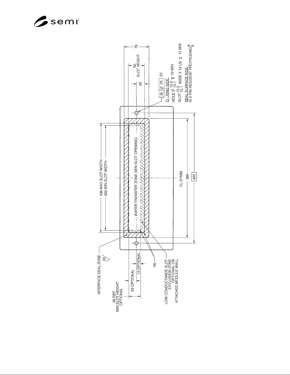
Inside Boundary Width-
Interface Seal Zone
2
236.0 mm (9.29
in.)
336.0 mm
(13.23 in.)
Outside Boundary Width-
Interface Seal Zone
2
266.0 mm
(10.47 in.)
366.0 mm
(14.41 in.)
Wafer Transfer Zone
Minimum Width
2
222.0 mm
(8.74 in.)
322.0 mm
(12.68 in.)
Alignment Pins Centerline
Separation
2
300.0 mm
(11.81 in.)
400.0 mm
(15.75 in.)
Flange Width
2
340.0 mm
(13.39 in.)
440.0 mm
(17.32 in.)
Vertical Slot Opening
(Inner boundary of Seal
Zone)
46 mm
(1.811 in.)
Maximum
50 mm
(1.969 in.)
Distance of Wafer Transfer
Plane above Alignment Pin
Datum Line (see Figure 1)
9.5 ± 0.5 mm
(0.37 ± 0.02 in.)
15.5 ± 0.5 mm
(0.61 ± 0.02 in.)
Vertical Motion Capability
(see Figure 1)
6 ± 0.5 mm
(0.24 ± 0.02 in.)
10 ± 0.5 mm
(0.39 ± 0.02 in.)
Minimum Distance of Slot
Top above Alignment Pin
Datum on Attached
Modules
(13 mm) 23 mm
(0.906 in.)
Minimum Distance of Slot
Bottom below Alignment
Pin Datum on Attached
Modules
(13 mm) 13 mm
(0.512 in.)
1. See Related Information R1-2.
2. See Related Information R1-3.
SEMI E21.1-1296 © SEMI 1992, 2002 2
Figure 1
Proposed 300 mm Wafer Transport Plane Elevation
SEMI E21.1-1296 © SEMI 1992, 2002 3
Figure 2
Proposed 300 mm Interface Plane