semi合集-English.pdf - 第172页
SEMI E21.1-1296 © SEMI 1992, 2002 4 NOTICE: SEMI makes no warranties or representatio ns as to the suitability of th e standards set forth herein for any particular application. Th e determination of the suitability of t…
SEMI E21.1-1296 © SEMI 1992, 2002 3
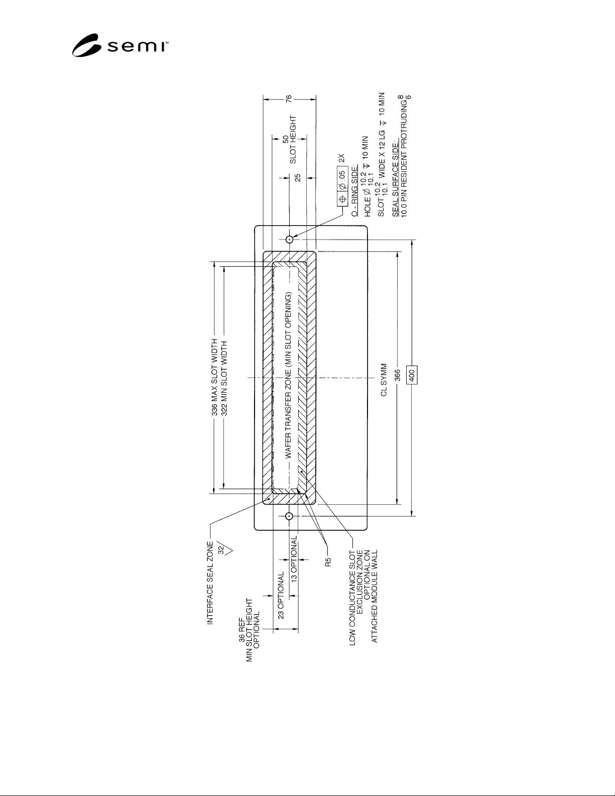
Figure 2
Proposed 300 mm Interface Plane

SEMI E21.1-1296 © SEMI 1992, 2002 4
NOTICE: SEMI makes no warranties or representations as to the suitability of the standards set forth herein for any
particular application. The determination of the suitability of the standard is solely the responsibility of the user.
Users are cautioned to refer to manufacturer' s instructions, product labels, product data sheets, and other relevant
literature, respecting any materials or equipment mentioned herein. These standards are subject to change without
notice.
The user’s attention is called to the possibility that compliance with this standard may require use of an invention
covered by patent rights. By publication of this standard, Semiconductor Equipment and Materials International
(SEMI) takes no position respecting the validity of any patent rights asserted in connection with any item mentioned
in this standard. In particular, users of the specification should be aware that Drytek, Inc., A Unit of General Signal,
16 Jonspin Road, Wilmington, MA 01887-1087, Phone: (508) 657-3933, has neither claimed nor disclaimed that
compliance with this specification would require use of an invention covered by one or more of its patents. Users of
this standard are expressly advised that determination of any such patent rights, and the risk of the infringement of
such rights, are entirely their own responsibility.

SEMI E21.1-1296 © SEMI 1992, 2002 5
RELATED INFORMATION 1
NOTE: The material contained in this related information is not an official part of SEMI E21.1, and is not meant to
modify or supersede it in any way. Rather, these notes are provided primarily as a source of information to aid in the
application of the standard. As such they are to be considered as reference material only. The standard should be
referred to in all cases.
R1-1 Vertical Requirements
R1-1.1 Changes in vertical requirements are made because of the need to provide adequate transport arm stiffness
(thickness) for the longer reach specified for 300 mm. However, for many processes, it is desirable to limit the slot
size as far as possible. An option is now allowed to reduce the vertical slot opening on the Attached Modules side of
the Interface Plane (see Figure 1, E21), but any such reduction will compromise the space otherwise available for
transport arm vertical thickness and/or movement. Specification of the extent of this option will be needed in each
case it is used.
R1-2 Transport Maximum Reach
A1-2.1 The maximum reach beyond the interface plane (see Table 1) is increased by 75 mm (from 305.0 mm to
380.0 mm); a 50 mm increase in wafer radius (from 100 mm to 150 mm) and a 25 mm increase in clearance between
the wafer and the chamber walls.
R1-3 Width Requirements
R1-3.1 The increase in wafer diameter from 200 mm to 300 mm necessitates a 100 mm increase in all width values
(see Table 1) specified in SEMI E21.
NOTICE: SEMI makes no warranties or representations as to the suitability of the standards set forth herein for any
particular application. The determination of the suitability of the standard is solely the responsibility of the user.
Users are cautioned to refer to manufacturer' s instructions, product labels, product data sheets, and other relevant
literature, respecting any materials or equipment mentioned herein. These standards are subject to change without
notice.
The user’s attention is called to the possibility that compliance with this standard may require use of an invention
covered by patent rights. By publication of this standard, Semiconductor Equipment and Materials International
(SEMI) takes no position respecting the validity of any patent rights asserted in connection with any item mentioned
in this standard. In particular, users of the specification should be aware that Drytek, Inc., A Unit of General Signal,
16 Jonspin Road, Wilmington, MA 01887-1087, Phone: (508) 657-3933, has neither claimed nor disclaimed that
compliance with this specification would require use of an invention covered by one or more of its patents. Users of
this standard are expressly advised that determination of any such patent rights, and the risk of the infringement of
such rights, are entirely their own responsibility.
Copyright by SEMI® (Semiconductor Equipment and Materials
International), 3081 Zanker Road, San Jose, CA 95134. Reproduction o
f
the contents in whole or in part is forbidden without express written
consent of SEMI.