semi合集-English.pdf - 第20页
SEMI E1.5-91 © SEMI 1984, 2003 2 Figure 6 150 mm Plastic & Metal Wafer Carrier General Usage NOTICE: SEMI makes no warranties or representatio ns as to the suitability of th e standards set forth herein for any parti…
SEMI E1.5-91 © SEMI 1984, 2003 1
SEMI E1.5-91 (Reapproved 1102)
E
STANDARD FOR 150 mm PLASTIC AND METAL WAFER CARRIERS,
GENERAL USAGE
This standard was technically approved by the Global Physical Interfaces and Carriers Committee and is the
direct responsibility of the North American Physical Interfaces and Carriers Committee. Current edition
approved by the North American Physical Interfaces and Carriers Committee on July 21, 2002. Initially
available at www.semi.org October 2002; to be published November 2002. Orignally published in 1984;
previously published February 1999.
E
This document was editorially modified in January 2003 to correct editorial errors that were introduced
into the document in earlier editions. Changes were made to the table header and the last two rows of the
table.
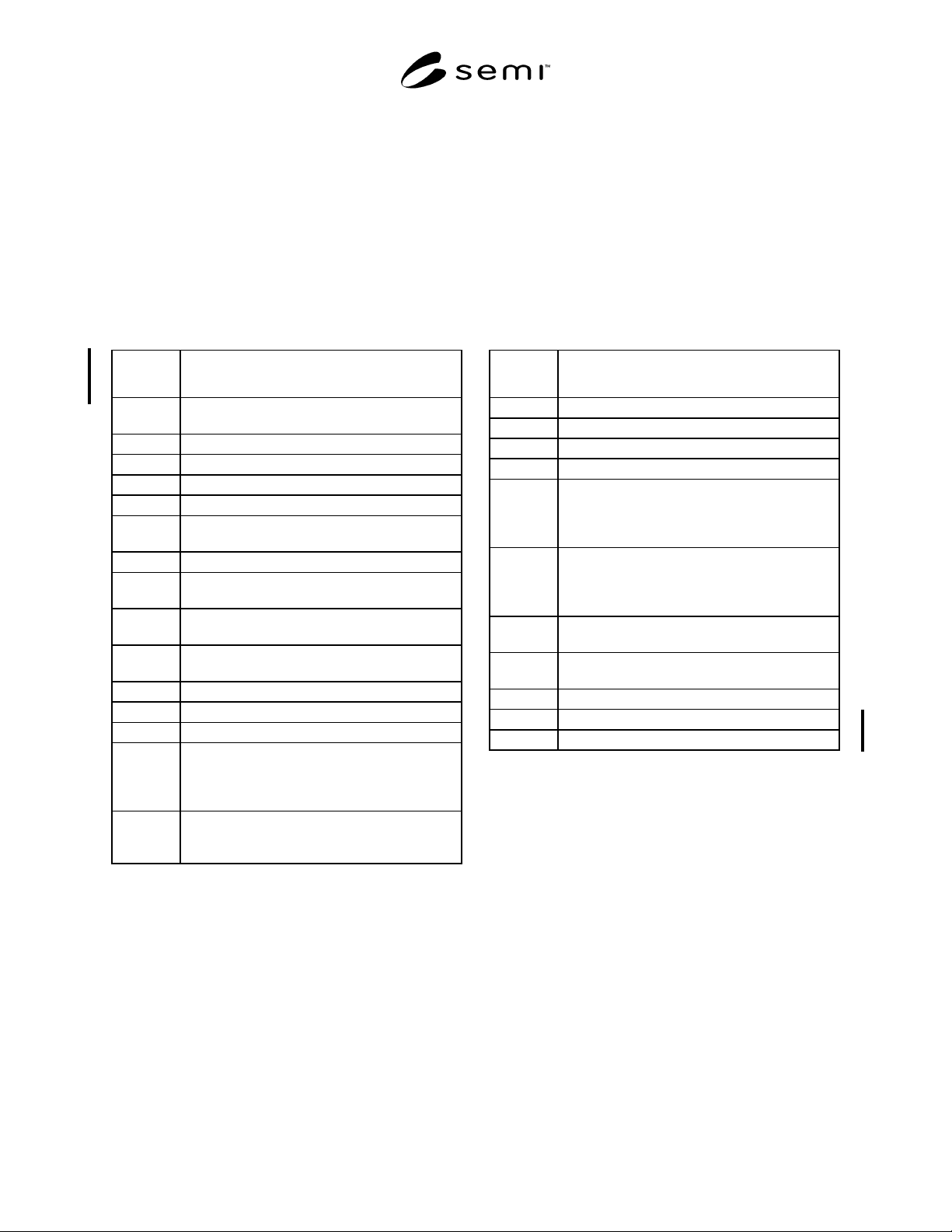
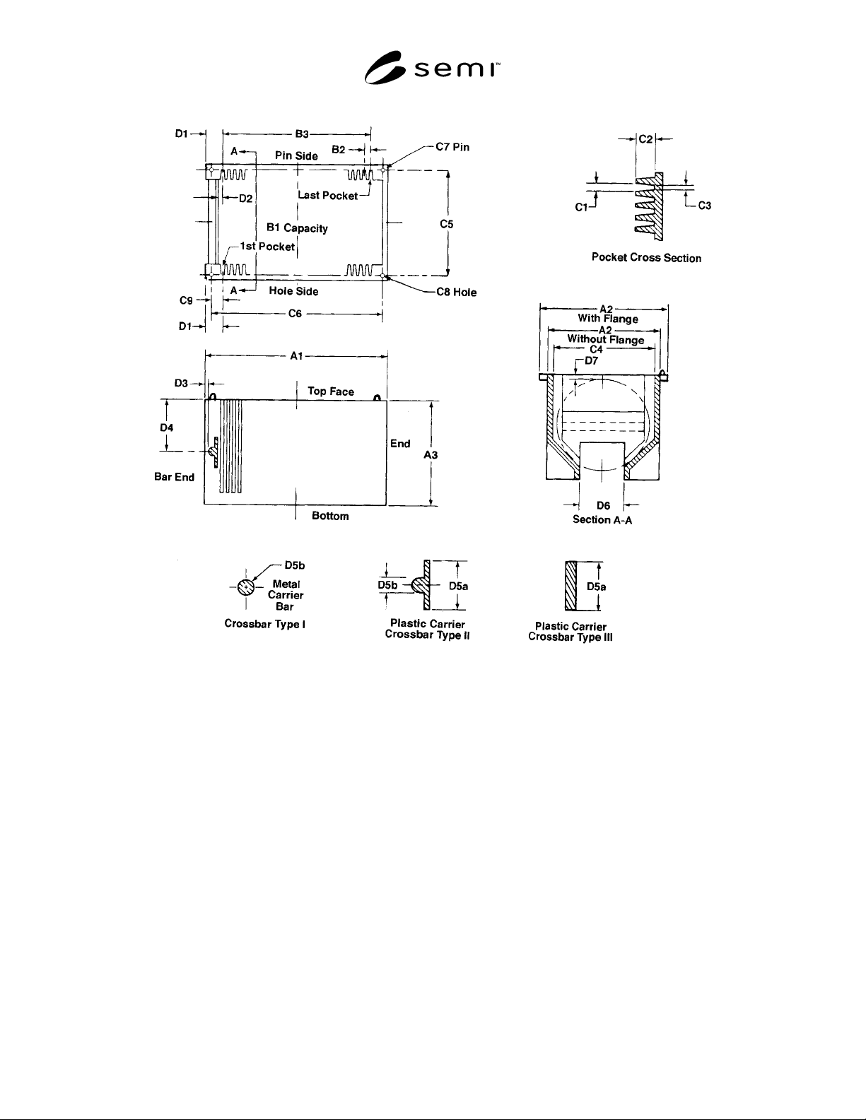
Figure 6
Reference
Overall Dimensions
A1 143.4 mm + 0.64 mm/– 0.5 mm
(5.645 inch + 0.025 inch/– 0.020 inch)
A2 177.80 mm (7.000 inch) maximum
A3 171.40 mm (6.750 inch) maximum
B1 25
B2 4.76 mm ± 0.25 mm (0.1875 inch ± 0.010 inch)
B3 114.30 mm ± 0.025 mm
(4.500 inch ± 0.010 inch)
C1 (C3) + 0.50 mm (0.020 inch) minimum
C2 9.53 mm (0.375 inch) minimum /
12.70 mm (0.500 inch) maximum
C3 1.52 mm ± 0.13 mm (0.060 inch ± 0.005 inch)
for plastic
2.03 mm + 0.00 mm/– 0.50 mm (0.080 inch +
0.000 inch/– 0.020 inch) for metal
C4 153.5 mm ± 1.0 mm (6.043 inch ± 0.040 inch)
C5 156.0 mm ± 0.5 mm (6.142 inch ± 0.020 inch)
C6 134.52 mm ± 0.25 mm (5.296 inch ± 0.010 inch)
C7 3.56 mm + 0.13 mm/– 0.38 mm (0.140 inch +
0.005 inch/– 0.015 inch) diameter by
4.32 mm ± 0.50 mm (0.170 inch ± 0.020 inch)
high
C8 3.96 mm + 0.50 mm/– 0.00 mm (0.156 inch +
0.020 inch/– 0.000 inch) diameter by
5.0 mm (0.197 inch) minimum depth
Figure 6
Reference
Overall Dimensions
C9 10.11 mm ± 0.25 mm (0.398 inch ± 0.010 inch)
D1 14.54 mm ± 0.25 mm (0.572 inch ± 0.010 inch)
D2 4.57 mm (0.18 inch) minimum
D3 1.57 mm ± 0.5 mm (0.062 inch ± 0.020 inch)
D4a 79.76 mm ± 0.50 mm (3.140 inch ± 0.020 inch)
This specification is applicable only to full-depth
wafer carriers, i.e., the wafer sits below the top o
f
the carrier.
D4b On center within ± 3.18 mm (± 0.125 inch)
This specification describes the center point of
the wafer in relationship to the centerline of the
crossbar (for a 150 mm nominal wafer).
D5a 25.40 mm + 0.0 mm/– 0.5 mm
(1.000 inch + 0.000 inch/– 0.020 inch)
D5b 6.35 mm + 0.00 mm/– 0.38 mm
(0.250 inch + 0.000 inch/– 0.020 inch)
D5c 4.45 mm ± 0.75 mm (0.175 inch ± 0.030 inch)
D6 76.2 mm (3.000 inch) minimum
Wafer Tilt 0.64 mm (0.025 inch) maximum
Usage Note: Because of the range of wafer carrier designs and wafer
carrier feature tolerances allowed by this standard, and because of the
range of wafer shapes and tolerances allowed by the wafer
dimensional standards, not every possible SEMI Standards wafer
carrier is compatible with every possible SEMI Standard wafer.
Please verify the compatibility of your specific wafer and carrier with
the respective vendors.
SEMI E1.5-91 © SEMI 1984, 2003 2
Figure 6
150 mm Plastic & Metal Wafer Carrier General Usage
NOTICE: SEMI makes no warranties or representations as to the suitability of the standards set forth herein for any
particular application. The determination of the suitability of the standard is solely the responsibility of the user.
Users are cautioned to refer to manufacturer’s instructions, product labels, product data sheets, and other relevant
literature respecting any materials mentioned herein. These standards are subject to change without notice.
The user’s attention is called to the possibility that compliance with this standard may require use of copyrighted
material or of an invention covered by patent rights. By publication of this standard, SEMI takes no position
respecting the validity of any patent rights or copyrights asserted in connection with any item mentioned in this
standard. Users of this standard are expressly advised that determination of any such patent rights or copyrights, and
the risk of infringement of such rights, are entirely their own responsibility.
Copyright by SEMI® (Semiconductor Equipment and Materials
International), 3081 Zanker Road, San Jose, CA 95134. Reproduction o
f
the contents in whole or in part is forbidden without express written
consent of SEMI.

SEMI E1.9-0701
E2
© SEMI 1994, 2004 1
SEMI E1.9-0701
E2
MECHANICAL SPECIFICATION FOR CASSETTES USED TO
TRANSPORT AND STORE 300 mm WAFERS
This specification was technically approved by the Global Physical Interfaces & Carriers Committee and is
the direct responsibility of the North American Physical Interfaces & Carriers Committee. Current edition
approved by the North American Regional Standards Committee on March 22 and April 30, 2001. Initially
available at www.semi.org May 2001; to be published July 2001. Originally published in 1994; previously
published June 1999.
E
This document was editorially modified in January 2003 to reflect the withdrawal of SEMI E44. Changes
were made to Sections 3.1, 4.2, 4.4, and 4.17. This document was also editorially modified in May 2004 to
reflect the withdrawal of SEMI E19.5. Changes were made to Section 7.1.
1 Purpose
1.1 This standard specifies the cassettes used to
transport and store 300 mm wafers in an IC
manufacturing facility. This includes both manual and
auto-transport use as well as high-speed extraction of
the wafers in processing equipment.
2 Scope
2.1 This standard is intended to set an appropriate level
of specification that places minimal limits on
innovation while ensuring modularity and
interchangeability at all mechanical interfaces. Most of
the requirements given in this specification are in the
form of maximum or minimum dimensions wit very
few required surfaces. Only the mechanical interfaces
for cassettes are specified; no materials requirements or
micro-contamination limits are given. However, this
standard has been written so that both metal and
injection-molded plastic cassettes can be manufactured
in conformance with it.
2.2 The cassette has the following components and
sub-components, and other features. A “† ” symbol
indicates components or features that include
dimensions required for boxes with non-removable
cassettes.
Key:
• Required feature
◊ Optional feature
• 1 top domain
• 2 optical wafer sensing paths
◊ 4 robotic handling flanges (optional)
◊ 1 top cassette identification tag area (optional)
• 2 or 4 side domains (2 in front and 2 in rear, if
needed)
• supports (for 13 or 25 wafers) with correct wafer
pitch (10 mm) †
• 1 optical cassette sensing hole on each front side
domain
◊ 1 side cassette identification tag area on front
right side domain only (optional)
◊ features that prevent wafer creep-out
(optional)
◊ 2 pentagonal side grip pits on each front side
domain (optional)
• 1 bottom domain
• 2 optical wafer sensing paths
• 5 carrier sensing pads †
• 4 info pads †
• 1 pod latch-pin hole
• 2 conveyor rails
• 2 fork-lift pick-up areas
• 2 fork-lift pin holes
• 3 features that mate with kinematic coupling pins
and provide a 10 mm lead in †
◊ 3 features that mate with kinematic coupling
pins and provide a 15 mm lead in (optional)
◊ 1 bottom cassette identification tag area
(optional)
• Other features
• multiple horizontal wafer sensing paths
• 2 end-effector exclusion zones †
3 Referenced Documents
3.1 SEMI Standards
SEMI E15 — Specification for Tool Load Port