semi合集-English.pdf - 第266页
SEMI E43-0301 © SEMI 1995 , 2001 14 RELATED INFORM A TI ON 3 ESD DA M AGE SIMULA TORS NOT E: T his relate d information is not an of ficial part of this standa rd. How ever, it contai ns relevant inf ormation f or using …
SEMI E43-0301 © SEMI 1995, 200113
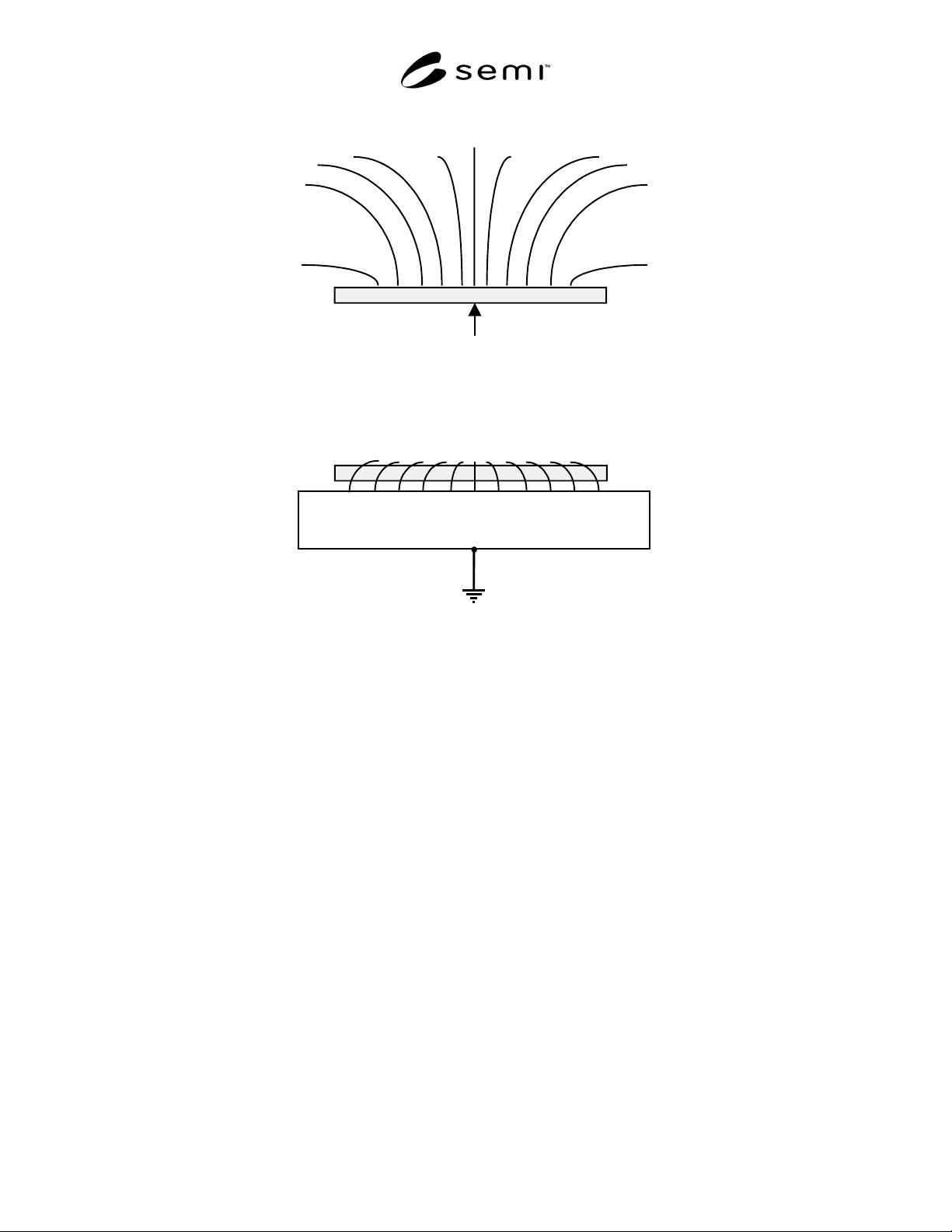
+ + + + + + + + + + + + +
Grounded Surface
Field Lines Terminate on Ground
and Do Not Accurately
Represent Charge on the Surface
Charged Surface
Field Lines Due to Static Charge
+ + + + + + + + + + + + + + + + +
Figure R2-1
Field Suppression

SEMI E43-0301 © SEMI 1995, 2001 14
RELATED INFORMATION 3
ESD DAMAGE SIMULATORS
NOTE: This related information is not an official part of this standard. However, it contains relevant information for using the
standard in situations commonly encountered with semiconductor manufacturing facilities and equipment. Determination of the
suitability of the material is solely the responsibility of the user.
R3-1 ESD Damage Simulators
R3-1.1 ESD Simulators are used to replicate ESD
events. Common types used to characterize
semiconductor devices and equipment include:
• Component Level HBM ESD Simulator.
• Component Level MM ESD Simulator.
• Component Level CDM ESD Simulator
• System Level HBM/metal ESD Simulator
R3-1.2 The component level HBM ESD Simulator
represents the parameters agreed upon for a standard,
which represents the discharge from a typical human
body. These parameters are 1500 ohms and 100 pF for
the representative resistance and capacitance
respectively of the human body.
R3-1.3 The component level MM ESD Simulator
represents the parameters agreed upon for a standard,
which represents the discharge from a charged metallic
arm of a machine (automatic handler etc). These
parameters are 200 pF and zero resistance for the
representative capacitance and DC resistance
respectively of the machine. We note here that the
resulting waveform is dependent on the impedance of
the circuity.
R3-1.4 The component level CDM ESD Simulator
represents the parameters agreed upon for a standard,
which represents the discharge from a charged device.
These parameters are defined by the resulting
waveform and depend almost exclusively on the
capacitance, resistance and inductance of each device
relative to ground. These parameters must not be
confused with the equipment parameters, which affects
the resulting waveform.
R3-1.5 The system level HBM/metal ESD Simulator
represents the parameters agreed upon for a standard,
which represents the discharge from a human holding a
metallic instrument. These parameters are the lower
resistance 350 ohms and 150 pF for the representative
resistance and capacitance respectively of the human
holding a metallic instrument. Note here that the
waveform is greatly affected by the equipment
parasitics.
R3.1.6 The above component level ESD simulators
have also been used in simulating ESD damage to
tooling, such as reticles and photomasks. This
simulation is left to user discretion.
R3-2 Summary of procedures
R3-2.1 HBM ESD Simulator-component level — The
procedure for using this simulator to stress test devices
or wafers is based upon the standard requirements.
ANSI and the ESD Association approved the HBM
standard, ESD STM5.1, which contains a specific
device pin combination sequence for stress testing.
This test procedure is generally referred to as a Pin to
Ground test since one pin is always grounded while the
selected second pin is stressed. Calibration before use
requires added equipment components like a current
probe, high bandpass cable, a short wire, a 500 ohm
resistor and a very high band width waveform
recorder/digitizer.
R3-2.2 MM ESD Simulator-component level — The
procedure for using this simulator to stress test devices
or wafers is based upon the standard requirements. The
ESD S5.2 approved MM standard specifies a specific
device pin combination sequence for stress testing.
This test procedure is also generally referred to as a Pin
to Ground test since one pin is always grounded while
the selected second pin is stressed. This procedure is
exactly the same as for HBM. Calibration before use
requires added equipment components like a current
probe, high bandpass cable, short wire, a 500 ohm
resistor and a very high band width waveform
recorder/digitizer.
R3-2.3 CDM ESD Simulator-component level — The
procedure for using this simulator to stress test devices
or wafers is based upon the standard requirements. The
ESD STM 5.3.1 approved CDM standard does not use a
pin combination procedure. Here the device sits on a
charge plate (CP) “dead-bug” style (package on CP and
leads/pins vertical) and each pin is discharged
successively after each charge to the device package.
This procedure is different from that of HBM and MM.
Calibration before use requires added equipment
components like a capacitance/inductance calibrator,
high bandpass cable and a very high band width
waveform recorder/digitizer.
R3-2.4 HBM-metal Simulator- system level — The
procedure for using this hand-held simulator for testing
systems (ATE testers, Automatic handlers, computers,
printers, ESD Simulators etc) is based upon the

SEMI E43-0301 © SEMI 1995, 200115
standard requirements. The IEC 61000-4-2, 1996
(formally-801-2,1992) standard uses direct contact or
air discharge to the system under test and is a different
procedure from the other three procedures mentioned
above. Calibration before use requires the use of a very
large vertical ground plane (at least 4 ft by 4 ft square),
a high BW current probe, cables and high bandwidth
waveform recorder/digitizer.
R3-3 Industry Classifications
R3-3.1 HBM classification
1. < 250 volts
2. 250 to < 500
3. 500 to < 1000
4. 1000 to < 2000
5. 2000 to < 4000
6. 4000 to < 8000
7. = or > 8000
R3-3.2 MM classification
1. M1 < 100
2. M2 100 to < 200
3. M3 200 to < 400
4. M4 400 to < 800
5. M5 = or > 800
R3-3.3 CDM classification
1. C1 < 125
2. C2 125 to < 250
3. C3 250 to < 500
4. C4 500 to < 1000
5. C5 1000 to < 2000
6. C6 = or > 2000
R3-3.4 Hand-Held Metal HBM classification
Direct Contact Discharge
Voltage Current
1. 2,000 12.0 amps
2. 4,000 24.0
3. 6,000 36.0
4. 8,000 48.0
Air Discharge
Voltage Current
1. 2,000 15.0 amps
2. 4,000 25.0
3. 6,000 30.0
4. 10,000 35.0
5. 15,000 52.0
Note that the currents for the same voltage level are not
the same for contact versus air discharge.