semi合集-English.pdf - 第3663页
SEMI E142-0705 © SEMI 2005 25 St r i p Wa f e r Orig inL o catio n( 0,0) = "L owe r L e ftT op" FX = 20 FY = 12 TX = 2 TY = 3 Figure R1-3 Strip Map Example – TransferMap NOTICE: SEMI makes no warranties or repr…
SEMI E142-0705 © SEMI 2005 24
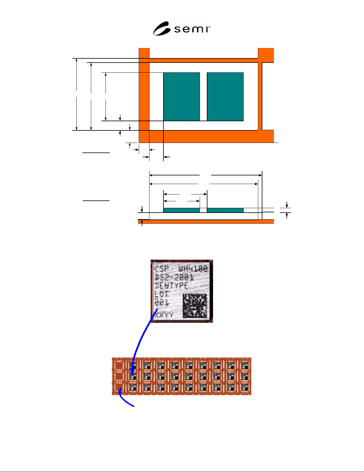
SRAM
FlashFlash
30.00
75.00
78.00
33.00
46.67
49.67
3.00
5.00
SRAM Layout
Dimension (X=32, Y =8)
LowerLef t (X=7.00, Y =8.33)
StepSize (X=78.00, Y=49.67)
Dev iceSize (X=75.00, Y =46.67)
Height = 5.00
ZOrder = 0
25.00
7.00
8.33
Flash Layout
Dimension (X=2, Y =1)
LowerLef t (X=10.00, Y=6.67)
StepSize (X=30.00, Y=0.00)
Dev iceSize (X=25.00, Y =33.0)
Height = 3.00
ZOrder = 1
6.67
10.00
Figure R1-1
Strip Map Example – Layout
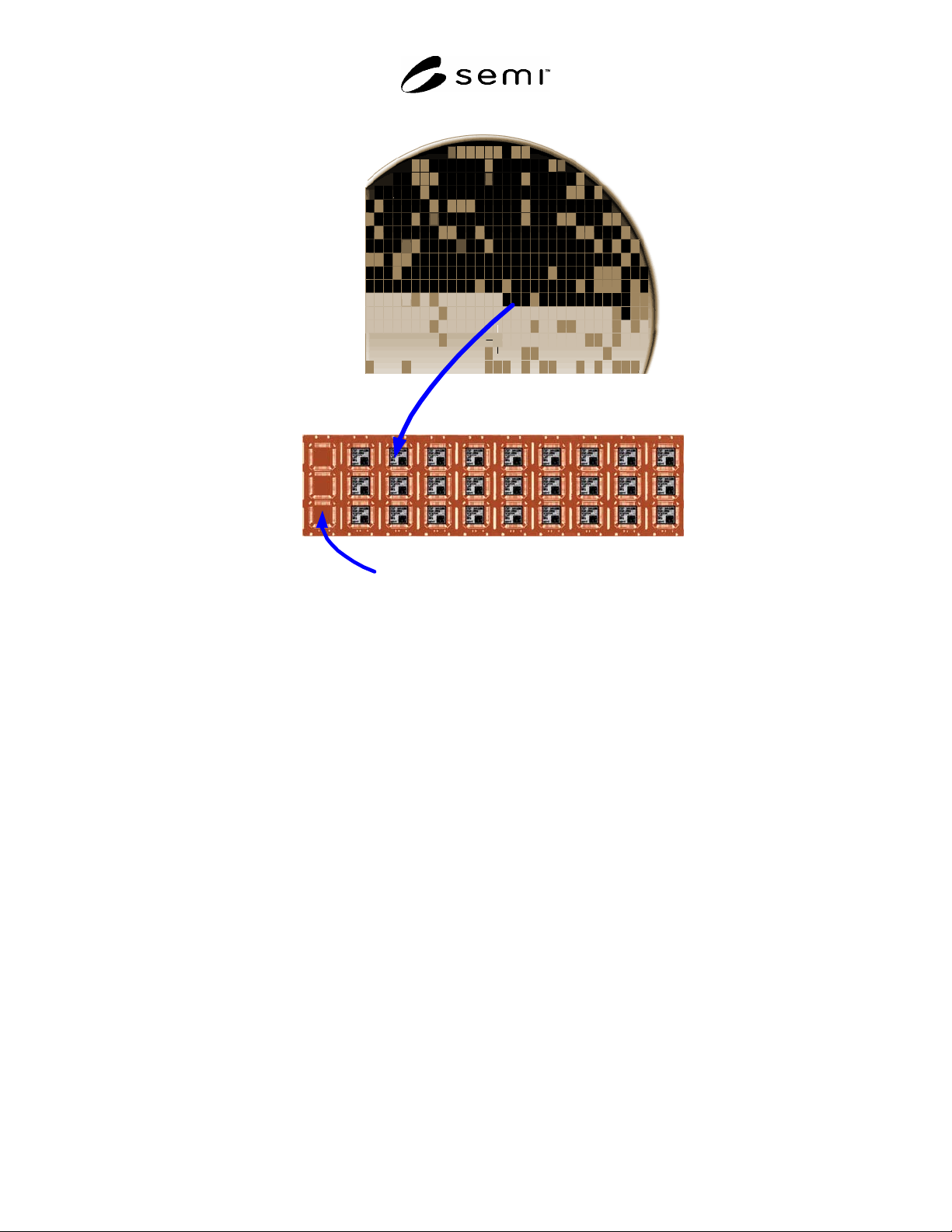
Strip
X = 1
Y = 1
OriginLocation (0,0) ="LowerLeftTop"
DeviceId
Figure R1-2
Strip Map Example – DeviceIdMap
SEMI E142-0705 © SEMI 2005 25
Strip
Wafer
OriginLocation(0,0) = "LowerLeftTop"
FX = 20
FY = 12
TX = 2
TY = 3
Figure R1-3
Strip Map Example – TransferMap
NOTICE: SEMI makes no warranties or representations as to the suitability of the standards set forth herein for any
particular application. The determination of the suitability of the standard is solely the responsibility of the user.
Users are cautioned to refer to manufacturer's instructions, product labels, product data sheets, and other relevant
literature, respecting any materials or equipment mentioned herein. These standards are subject to change without
notice.
By publication of this standard, Semiconductor Equipment and Materials International (SEMI) takes no position
respecting the validity of any patent rights or copyrights asserted in connection with any items mentioned in this
standard. Users of this standard are expressly advised that determination of any such patent rights or copyrights, and
the risk of infringement of such rights are entirely their own responsibility.
Copyright by SEMI® (Semiconductor Equipment and Materials
International), 3081 Zanker Road, San Jose, CA 95134. Reproduction of
the contents in whole or in part is forbidden without express written
consent of SEMI.
SEMI E142.1-0705 © SEMI 2005 1
SEMI E142.1-0705
XML SCHEMA FOR SUBSTRATE MAPPING
This standard was technically approved by the global Information & Control Committee. This edition was
approved for publication by the global Audits and Reviews Subcommittee on April 7, 2005. It was available
at www.semi.org in June 2005 and on CD-ROM in July 2005.
1 Purpose
1.1 The purpose of this specification is to provide an XML schema that corresponds to the data model for
equipment defined by SEMI E142, Specification for Substrate Mapping. This schema is available to equipment
communication standards that want to use SEMI E142 -defined information in XML formatted equipment
communication.
2 Scope
2.1 The scope of this document is the representation of the SEMI E142 object model in an XML schema. It will not
add new domain information or concepts to the model. The only additions made are those needed to render a useful
XML schema.
NOTICE: This standard does not purport to address safety issues, if any, associated with its use. It is the
responsibility of the users of this standard to establish appropriate safety and health practices and determine the
applicability of regulatory or other limitations prior to use.
3 Referenced Standards and Documents
3.1 SEMI Standards
SEMI E142 — Specification for Substrate Mapping
SEMI E121 — Guide for Style and Usage of XML for Semiconductor Manufacturing Applications
3.2 OMG Standards
Unified Modeling Language (UML) Specification, Version 1.4, OMG Specification 01-09-67,
(
http://www.omg.org/technology/documents/modeling_spec_catalog.htm
).
3.3 W3C Standards
Extensible Markup Language (XML) 1.0 (Second Edition) — W3C, 6 October 2000
(http://www.w3.org/TR/2000/REC-xml-20001006/).
Namespaces in XML — W3C, 14 January 1999 (http://www.w3.org/TR/1999/REC-xml-names-19990114/).
XML Schema Part 0: Primer — W3C, 2 May 2001 (http://www/w3/org/TR/xmlschema-0/).
XML Schema Part 1: Structures — W3C, 2 May 2001 (http://www/w3/org/TR/xmlschema-1/).
XML Schema Part 2: Datatypes — W3C, 2 May 2001 (http://www/w3/org/TR/xmlschema-2/).
XML Path Language (Xpath) — W3C, 16 November 1999 (http://www/w3/org/TR/xpath/).
4 Terminology
4.1 Abbreviations and Acronyms
4.2 UML — Unified Modeling Language
4.3 W3C — World Wide Web Consortium
4.4 XML — eXtensible Markup Language