semi合集-English.pdf - 第4157页
SEMI F66-1101 © SEMI 2001 1 SEMI F66-1101 SPECIFICA TION FOR PORT M A RK ING AND SYMBOL OF STA I NLESS STEEL VESSELS FOR L IQUID CHEMICA LS This spe cification w as technically approved by the Global L iquid Chemica l Di…
SEMI F65-1101 © SEMI 2001 2
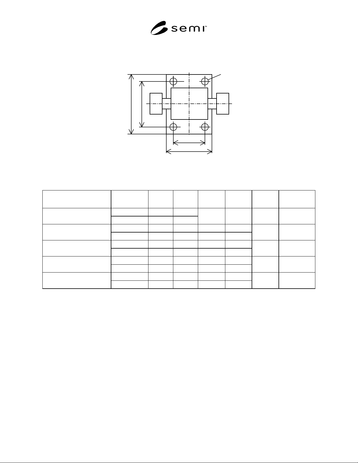
5.4 Where the dimension depends on the valve design considering the back pressure, the upper row in Table 1
applies to the valves that withstand up to 0.2 megapascals (MPa) (29 pounds per square inch (psi)) back pressure,
and the lower row applies to the valves that withstand more than 0.2 MPa (29 psi) back pressure.
φD
w’ w
l
l’
Figure 1
Top View of A Typical Diaphragm Valve with A Mounting Base
Table 1 Dimensional Specifications
Tube Size (mm) (OD / ID)* Back Pressure
(Mpa)
l’ (mm) l (mm) w’ (mm) w (mm)
φ
D (mm)
Bolt Type
(example)
≤ 0.2
60 48
25 / 22
> 0.2
68 56
96 84 7 M6
≤ 0.2
44 32 76 64
19 / 16
> 0.2
52 40 84 72
7
M6
≤ 0.2
34 22 62 50
12 / 10
> 0.2
46 34 70 58
7M6
≤ 0.2
34 22 62 50
10 / 8
> 0.2
46 34 68 56
7M6
≤ 0.2
32 20 56 44
6 / 4
> 0.2
40 28 60 48
7
M6
Note 1: OD and ID are outside diameter and inside diameter of the tube respectively.
Note 2: Refer to ISO 2768-1 or JIS B 0405 for tolerances.
6 Measurements
6.1 The mounting base must be conditioned for a minimum of one hour in an air environment of 23 ± 3ºC (73.4 ±
5.4ºF) prior to measuring the dimensions.
NOTICE: SEMI makes no warranties or representations as to the suitability of the standards set forth herein for any
particular application. The determination of the suitability of the standard is solely the responsibility of the user.
Users are cautioned to refer to manufacturer's instructions, product labels, product data sheets, and other relevant
literature, respecting any materials or equipment mentioned herein. These standards are subject to change without
notice.
By publication of this standard, Semiconductor Equipment and Materials International (SEMI) takes no position
respecting the validity of any patent rights or copyrights asserted in connection with any items mentioned in this
standard. Users of this standard are expressly advised that determination of any such patent rights or copyrights, and
the risk of infringement of such rights are entirely their own responsibility.
Copyright by SEMI® (Semiconductor Equipment and Materials
International), 3081 Zanker Road, San Jose, CA 95134. Reproduction o
f
the contents in whole or in part is forbidden without express written
consent of SEMI.
SEMI F66-1101 © SEMI 20011
SEMI F66-1101
SPECIFICATION FOR PORT MARKING AND SYMBOL OF STAINLESS
STEEL VESSELS FOR LIQUID CHEMICALS
This specification was technically approved by the Global Liquid Chemical Distribution Systems Committee
and is the direct responsibility of the Japanese Liquid Chemical Distribution Systems Committee. Current
edition approved by the Japanese Regional Standards Committee on August 3, 2001. Initially available at
www.semi.org September 2001; to be published November 2001.
1 Purpose
1.1 This document specifies port marking and symbol
of stainless steel vessels for liquid chemicals used in
semiconductor and flat panel display manufacturing
equipment and liquid chemical distribution facilities.
2 Scope
2.1 This document covers stainless steel vessels with
tubes that penetrate into the vessels as inlets or outlets
of liquid chemical to/from the vessels.
2.2 A vessel which uses coupling (quick coupling) at
its tube end (port) is excepted from the scope.
2.3 This standard does not purport to address safety
issues, if any, associated with its use. It is the
responsibility of the user of this standard to establish
appropriate safety and health practices and determine
the applicability of regulatory limitations prior to use.
3 Referenced Standards
3.1 None.
4 Terminology
4.1 dip tube — a piece of tube which penetrates into a
vessel as an inlet or outlet of liquid chemical to/from
the vessel.
4.2 liquid chemical — organic or inorganic liquid
chemical used for semiconductor or flat panel display
manufacturing.
4.3 port — an end of a tube attached to a vessel.
5 Requirements for Port Marking
5.1 The dip tube port shall be marked as “DIP”. If
more than one dip tube port exists on a vessel, each port
shall be marked as “DIP”.
5.2 Additional Marking — A description to identify
multiple ports may be added to the dip port marking
such as DIP-1 or DIP (1).
5.3 Location of Marking — “DIP” marking shall be
located where it will clearly identify the dip tube port.
If more than one dip tube ports exist on a vessel, each
marking shall be located so that the corresponding port
is clearly identified.
5.4 Method of Marking — The marking shall be
engraved, etched, or labeled properly so that the “DIP”
marking shall not be removed. Color of the marking is
optional.
5.5 Size of Marking — The marking shall be sized so
that it is clearly readable.
6 Requirements for Symbol
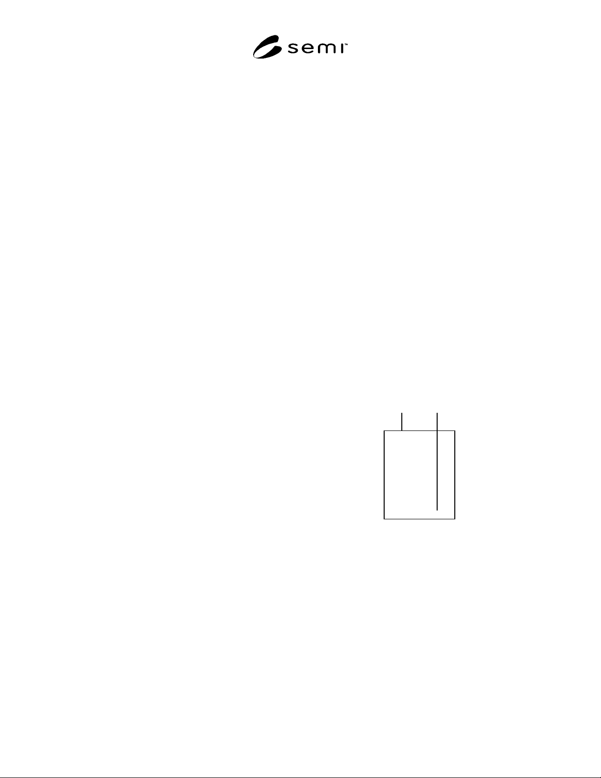
6.1 A symbol illustrated in Figure 1 shall be used to
draw a stainless steel vessel with a dip tube. A dip tube
shall be identified in the symbol as a line penetrating
into a rectangle.
6.2 If more than one dip tube exists on a vessel, the
symbol shall have the same number of lines which
correspond to the dip tubes.
Figure 1
Symbol for Stainless Steel Vessel with a Dip Tube
NOTICE: SEMI makes no warranties or
representations as to the suitability of the standards set
forth herein for any particular application. The
determination of the suitability of the standard is solely
the responsibility of the user. Users are cautioned to
refer to manufacturer' s instructions, product labels,
product data sheets, and other relevant literature,
respecting any materials or equipment mentioned
herein. These standards are subject to change without
notice.

SEMI F66-1101 © SEMI 2001 2
By publication of this standard, Semiconductor
Equipment and Materials International (SEMI) takes no
position respecting the validity of any patent rights or
copyrights asserted in connection with any items
mentioned in this standard. Users of this standard are
expressly advised that determination of any such patent
rights or copyrights, and the risk of infringement of
such rights are entirely their own responsibility.
Copyright by SEMI® (Semiconductor Equipment and Materials
International), 3081 Zanker Road, San Jose, CA 95134. Reproduction o
f
the contents in whole or in part is forbidden without express written
consent of SEMI.