semi合集-English.pdf - 第4199页
SEMI F73-1102 © SEMI 2002 1 SEMI F73-1102 TEST METHOD FOR SCANNING ELECTRON MICROSCOPY (SEM) EVALUATION OF WETTED SURFAC E CONDITION OF STAINLESS STEEL COMPONENTS This test method was technically approved b y the Global …
SEMI F72-1102 © SEMI 2002 9
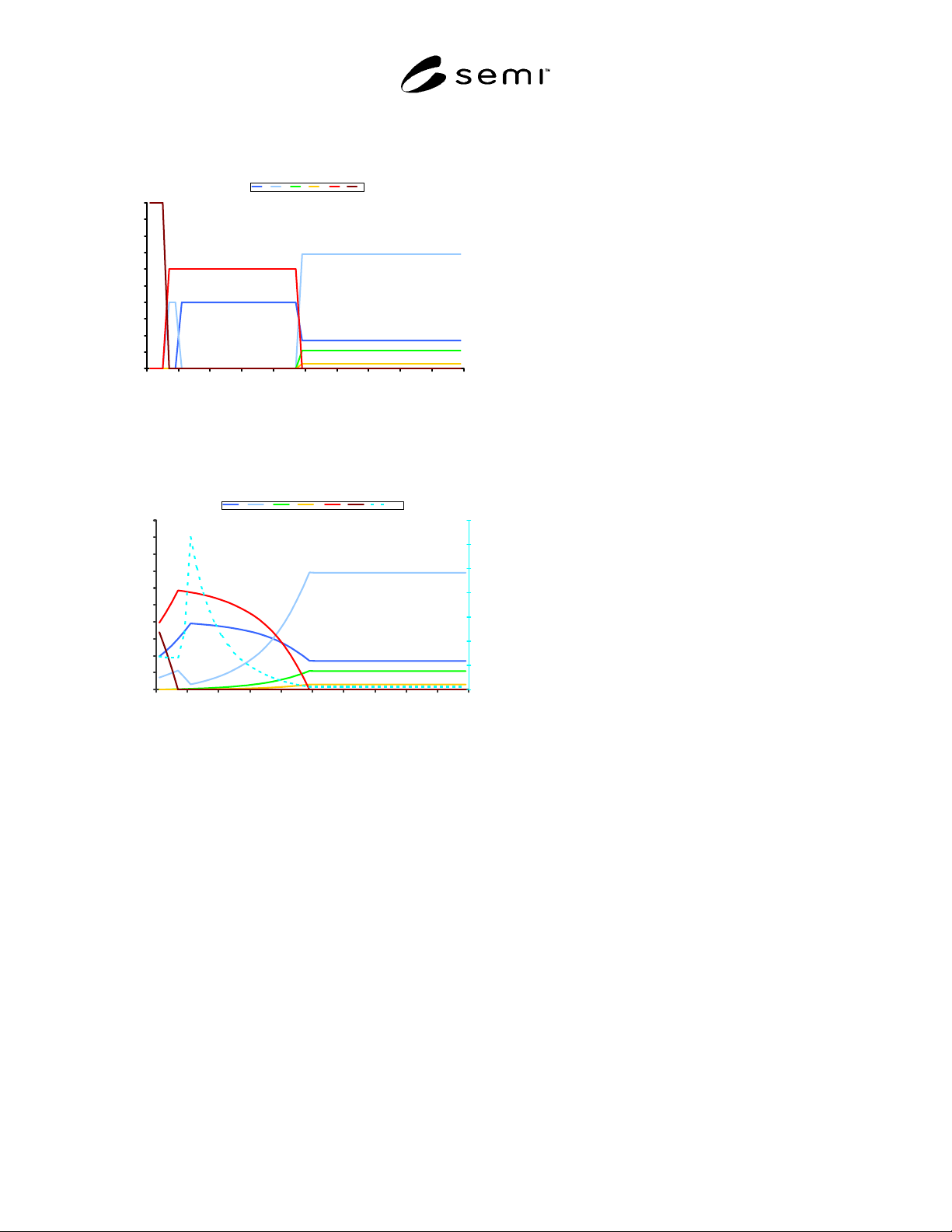
the presence of the carbon layer and the depth of
analysis.
Theoretical
0
10
20
30
40
50
60
70
80
90
100
0 5 10 15 20 25 30 35 40 45
Angstroms
Atomic Concentration
Cr Fe Ni Mo O C
Figure A1-10
Composition Versus Depth of a Carbon Layer Over
a Fe
2
O
3
Layer Over a Cr
2
O
3
Layer on Stainless Steel
Convoluted 5 Lambda
0
10
20
30
40
50
60
70
80
90
100
0 5 10 15 20 25 30 35 40 45
Angstroms
Atomic Concentration
0
2
4
6
8
10
12
14
Cr Fe Ni Mo O C Cr:Fe
Figure A1-11
Theoretical Depth Profile of Figure 11 Assuming 5λ
Depth of Analysis
A1-8
A1-8.1 It must be emphasized that these derived depth
profiles are for models with perfect interfaces and
perfect compositions instead of the compositional
gradients observed in real systems. Additional
measurement uncertainties result from roughness and
non-planarity of the surface, and from differential
sputtering rates for different chemical species during
depth profiling.
A1-8.2 The depth profiles of real systems must be
interpreted with an understanding of the effects
described in this appendix and a realization that they
are not ideal. The same considerations pertain to ESCA
depth profile analysis.
NOTICE: SEMI makes no warranties or
representations as to the suitability of the standards set
forth herein for any particular application. The
determination of the suitability of the standard is solely
the responsibility of the user. Users are cautioned to
refer to manufacturer's instructions, product labels,
product data sheets, and other relevant literature,
respecting any materials or equipment mentioned
herein. These standards are subject to change without
notice.
By publication of this standard, Semiconductor
Equipment and Materials International (SEMI) takes no
position respecting the validity of any patent rights or
copyrights asserted in connection with any items
mentioned in this standard. Users of this standard are
expressly advised that determination of any such patent
rights or copyrights, and the risk of infringement of
such rights are entirely their own responsibility.
Copyright by SEMI® (Semiconductor Equipment and Materials
International), 3081 Zanker Road, San Jose, CA 95134. Reproduction o
f
the contents in whole or in part is forbidden without express written
consent of SEMI.

SEMI F73-1102 © SEMI 2002 1
SEMI F73-1102
TEST METHOD FOR SCANNING ELECTRON MICROSCOPY (SEM)
EVALUATION OF WETTED SURFACE CONDITION OF STAINLESS
STEEL COMPONENTS
This test method was technically approved by the Global Gases Committee and is the direct responsibility of
the North American Gases Committee. Current edition approved by the North American Regional Standards
Committee on August 29, 2002. Initially available at www.semi.org September 2002; to be published
November 2002.
1 Purpose
1.1 This document defines a uniform procedure for
testing the wetted surfaces of stainless steel components
intended for installation into high purity gas distribution
systems. This procedure characterizes the occurrence,
frequency, and in some cases the identity of
microscopic surface defects and contaminants that may
appear on the wetted surfaces. It should be noted that
there has been no direct correlation made between the
results of this test method and contamination of process
gases or product yields in processes served by high
purity gas distribution systems. Application of this test
method is intended to yield comparable and
reproducible results among various users of this method
for the purposes of qualification of components.
1.2 The objective of this method is to describe a
general set of instrument parameters and conditions that
will achieve precise and reproducible measurements of
important parameters regarding the surface condition.
2 Scope
2.1 This procedure applies to the wetted surfaces in
stainless steel tubing, fittings, valves, and other
components to determine the effectiveness of surface
finishing and cleaning processes. The technique
describes counting of surface defects including pits,
inclusions, inclusion stringers, scratches, residual
process marks, grain boundaries and contamination on
the wetted surfaces. However, any surface damage
produced during sample preparation is to be excluded
from such assessment.
2.2 This standard does not purport to address safety
issues, if any, associated with its use. It is the
responsibility of the users of this standard to establish
appropriate safety health practices and determine the
applicability or regulatory limitations prior to use.
3 Limitations
3.1 This test method is primarily intended to determine
the frequency of occurrence (surface density) and
identity of microscopic surface defects, down to a size
range of ≥ approximately 0.1 micrometer, that may be
detrimental to high purity gas distribution systems.
Such defects may not be identifiable by visual or
magnified optical inspection, but concentrations of
microscopic surface defects may cause visually
apparent defects such as haze.
3.2 This test method requires sectioning of the
specimen(s) used for test purposes and is therefore
destructive.
3.3 The method must be applied to representative
examples of process lots to determine quality of the
processes employed and/or lots processed. As the areas
examined and measured by this method are very small,
the results may not be representative of all areas or all
lots processed.
3.4 This test method may be subject to operator bias in
selection of representative areas and definition of
countable defects.
3.5 Detection of countable defects is affected by
operator selection of SEM operating conditions and
image recording conditions. This test method assumes
that the operator is sufficiently proficient in operation
of the SEM to minimize this limitation, per instructions
in the procedures.
3.6 SEM imaging will reveal surface finish flaws, but
may not show features that are well rounded by an
electropolishing or other surface leveling process.
3.7 Energy dispersive X-ray spectroscopy (EDS) may
be used in this test method to analyze surface
contaminants at least approximately one micrometer in
thickness and inclusions at least approximately one
micrometer in size. EDS is not an appropriate
technique for analysis of the oxide passive layer on the
stainless steel surface, as EDS analyzes down to a depth
of the order of 1 micrometer below the surface, and the
oxide passive layer is only 0.001 to 0.01 micrometer
deep.

SEMI F73-1102 © SEMI 2002 2
4 Referenced Standards
4.1 ASTM Standards
1
ASTM E 7 — Standard Terminology Relating to
Metallography
ASTM E 766 — Standard Practice for Calibrating the
Magnification of a Scanning Electron Microscope
4.2 ANSI
2
/IEEE Standard
3
759 —Standard Test Procedures for Semiconductor X-
ray Energy Spectrometers
NOTE 1: Unless otherwise indicated, all documents cited
shall be the latest published versions.
5 Terminology
5.1 Abbreviations and Acronyms
5.1.1 EDS — Energy Dispersive X-ray spectroscopy,
sometimes called EDX.
5.1.2 FWHM — abbreviation of Full Width Half
Maximum; the width of an EDS peak measured at half
its maximum height.
5.1.3 SEM — Scanning Electron Microscopy.
5.2 Definitions
5.2.1 defect — any surface feature that is either
characteristic of the material, or a result of material
processing or product fabrication, that is deemed
capable of generating and/or trapping and releasing
particles, or otherwise be detrimental to the contained
fluids. Specific features that may be considered to be
defects, with definitions that relate to the purposes of
this document and/or obtained from reference sources
noted include:
5.2.1.1 contamination — three dimensional alien
material adhering to a surface. (SEMI Compilation of
Terms)
5.2.1.2 grain boundary — an interface separating two
grains, where the orientation of the lattice changes from
that of one grain to that of the other. (ASTM E 7)
5.2.1.3 inclusion — indigenous or foreign material
within the metal, usually referring to non-metallic
1 American Society for Testing and Materials, 100 Barr Harbor
Drive, West Conshohocken, Pennsylvania 19428-2959, USA.
Telephone: 610.832.9585, Fax: 610.832.9555 Website:
www.astm.org
2 American National Standards Institute, New York Office: 11 West
42nd Street, New York, NY 10036, USA. Telephone: 212.642.4900;
Fax: 212.398.0023 Website: www.ansi.org
3 Institute of Electrical and Electronics Engineers, IEEE Operations
Center, 445 Hoes Lane, P.O. Box 1331, Piscataway, New Jersey
08855-1331, USA. Telephone: 732.981.0060; Fax: 732.981.1721
compound particles such as oxides, alumina, sulfides or
silicates.
5.2.1.4 pit — a surface cavity or crater with a defined
edge not caused by impact.
5.2.1.5 process marks — a surface texture or pattern
that is characteristic of the surface finishing process
employed.
5.2.1.6 scratch — an elongated mark or groove cut in
the surface by mechanical means, not associated with
the predominant surface texture pattern. (adapted from
SEMI Compilation of Terms)
5.2.1.7 stringer — a microstructural configuration of
alloy constituents or foreign nonmetallic material, or
trace thereof, lined up in the direction of working.
(adapted from ASTM E 7)
5.2.2 wetted surface — surfaces of a component
contacting the contained fluids. (adapted from SEMI
Compilation of Terms)
5.2.3 working distance — the distance between the
surface of the specimen being examined and the front
surface of the objective lens. (ASTM E 7)
6 Summary of Method
6.1 Obtain a SEM photomicrograph of a representative
area of the wetted surface of the sample at a
magnification of 200×. Increase the magnification to
1000× and take another SEM photomicrograph within
this area, and another at a pre-selected magnification
within the range 3000 to 3600×. Obtain 3000–3600×
photomicrographs at two additional representative
areas, not necessarily within the 200× magnification
region.
6.2 If inclusions or contaminants are noted on any
3000–3600× magnification photos, EDS spectra of
representative example(s) may be obtained.
6.3 Perform grid overlay defect counting on the three
3000–3600× photos. Report results in tabular form;
provide photomicrographs and EDS spectra with
identification of elements detected.
7 Interferences
7.1 Interferences may be encountered as overlaps in
EDS spectral peaks. Specific overlaps that may be
encountered include but are not limited to:
7.1.1 Molybdenum and Sulfur — Overlap in EDS
spectra of Mo L peaks and S K peaks prevents
unambiguous determination.
7.1.2 Manganese and Chromium/Iron — Overlap in
EDS spectra of Mn Kα peak with Cr Kβ peak, and Mn