semi合集-English.pdf - 第430页
SEMI E57-0305 © SEMI 1996, 2005 6 RELATED INFORMATION 1 APPLICATION NOTES NOTICE : This relat ed information is not an offi cial part of SEMI E5 7. This relate d inform ation was approved for publication by full letter b…
SEMI E57-0305 © SEMI 1996, 2005 5
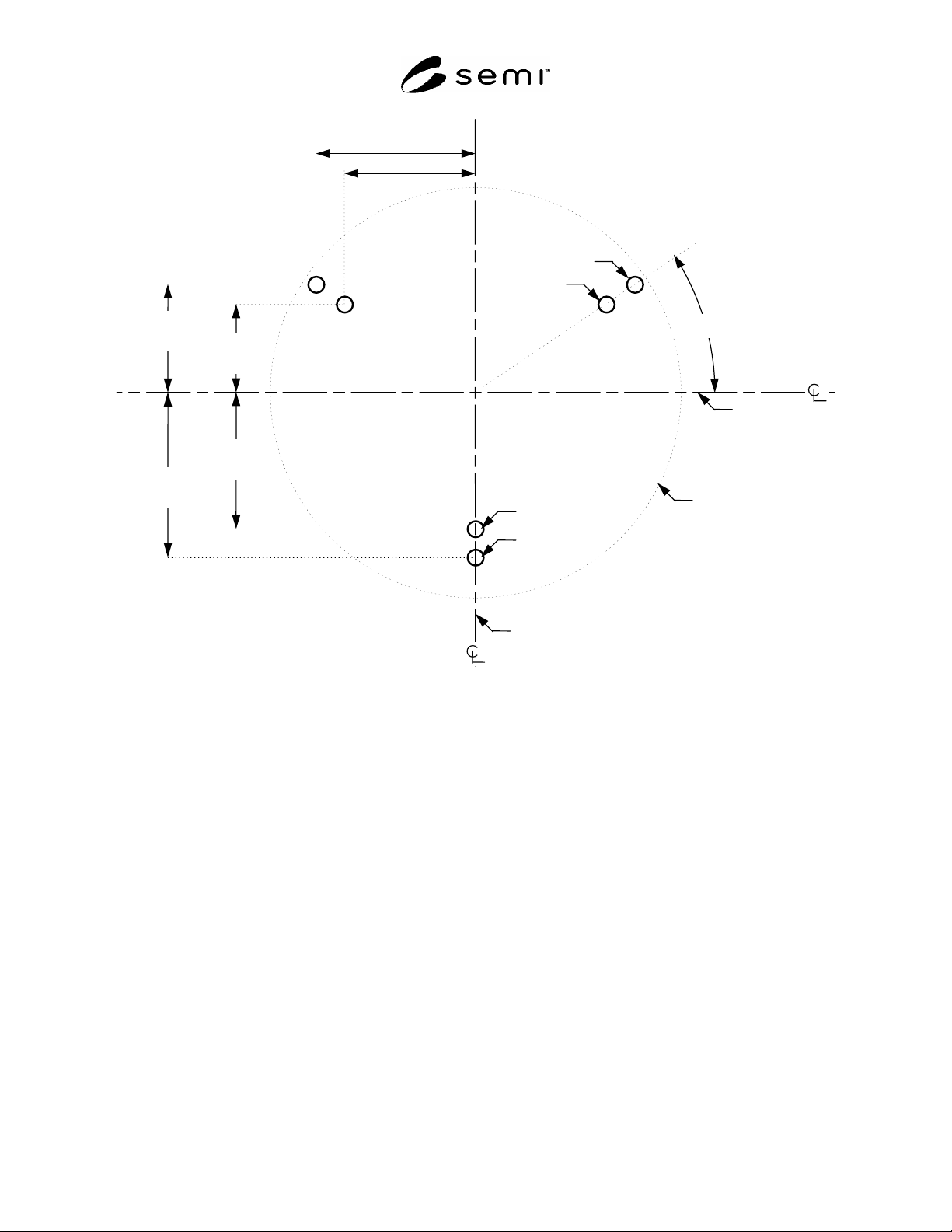
Figure 3
Kinematic Coupling Pin Locations
y 92
= 120 ± 0.05
y
93
= 64 ± 0.05
y 94
= 96 ± 0.05
y 91
= 80 ± 0.05
primary pin
facial
datum
plane
x
91 = 115 ± 0.05
x92
=92 ± 0.05
300-mm
wafer
bilateral datum plane
34.8°)
secondary pin
primary pin
secondary
pin
SEMI E57-0305 © SEMI 1996, 2005 6
RELATED INFORMATION 1
APPLICATION NOTES
NOTICE: This related information is not an official part of SEMI E57. This related information was approved for
publication by full letter ballot procedures.
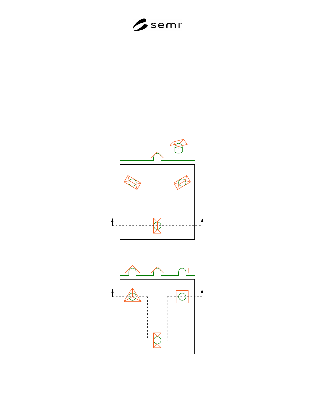
R1-1 The three features on the bottom of the wafer carrier that mate with the six pins underneath are not specified
in this standard. These three features are recommended to be inverted V-shaped grooves, each of which extends
along a line that is perpendicular to, and co-planar with, the nominal wafer center line (as shown in Figure R1-1).
Such grooves are likely to work well even when shrunken or slightly misaligned (such as when they do not all line
up with the nominal wafer center line). Other mating features are also possible, such as those shown in Figure R1-2
where one pin is contacted on the top. Front-opening boxes may need to contact the pins on the side to provide
pressure against a front mechanical interface. Such options are why the top and sides of the pins are toleranced so
tightly. When designing the mating features on the bottom of the wafer carrier, it is suggested that designers follow
the recommendations given in the book (listed in §6) by Dr. Alexander H. Slocum.
Figure R1-1
Recommended Mating Features
Figure R1-2
Alternative Mating Features
SEMI E57-0305 © SEMI 1996, 2005 7
R1-2 All of the dimensions for the kinematic coupling pin surfaces and locations are given as ranges so that any
roundness, cylindricity, perpendicularity, bending, or misalignment of the pins must be contained within the limits
given.
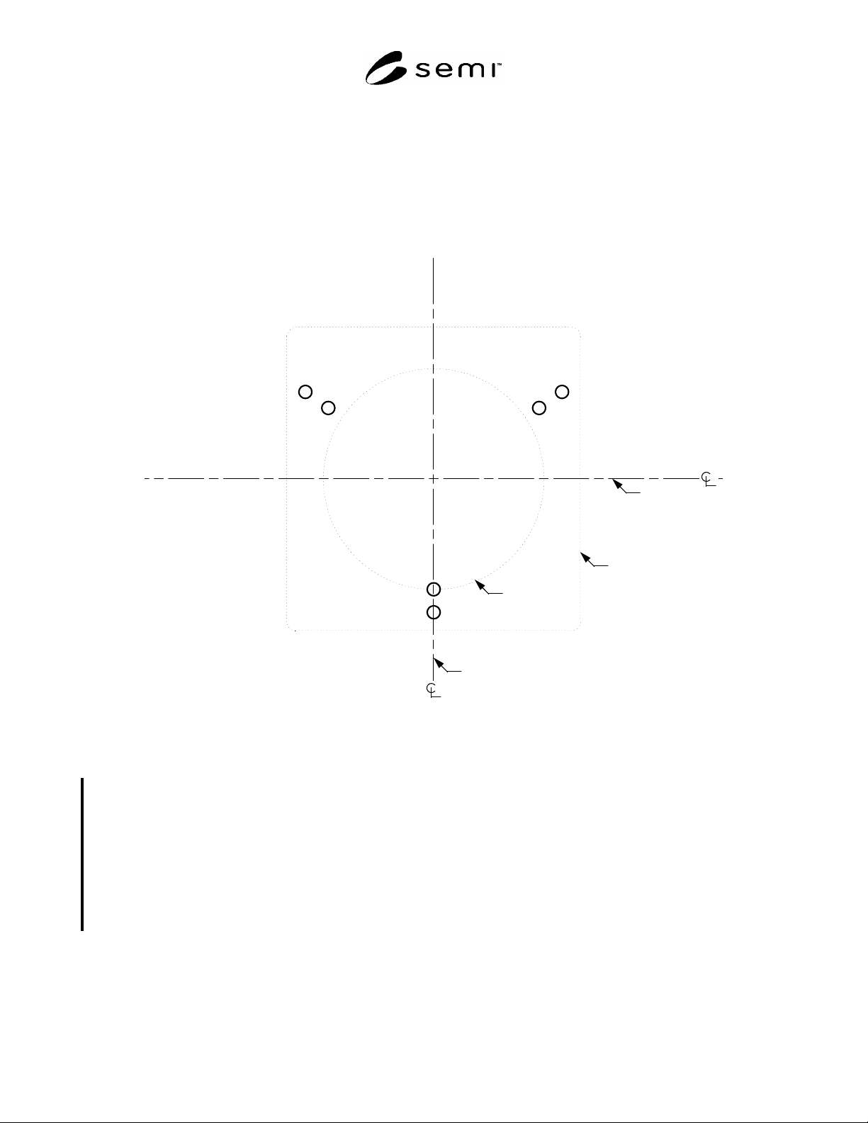
R1-3 As shown in Figure R1-3, these couplings can also be used to support 200 mm pods as an addition to the
requirements given in SEMI E19.4. However, concurrent implementations for both 200 and 300 mm wafer carriers
may be covered by patent claims.
facial
datum
plane
bilateral datum plane
200-mm
wafer
200-mm
SMIF
pod door
Figure R1-3
Application to 200 mm Pods
NOTICE: SEMI makes no warranties or representations as to the suitability of the standards set forth herein for any
particular application. The determination of the suitability of the standard is solely the responsibility of the user.
Users are cautioned to refer to manufacturer's instructions, product labels, product data sheets, and other relevant
literature, respecting any materials or equipment mentioned herein. These standards are subject to change without
notice.
By publication of this standard, Semiconductor Equipment and Materials International (SEMI) takes no position
respecting the validity of any patent rights or copyrights asserted in connection with any items mentioned in this
standard. Users of this standard are expressly advised that determination of any such patent rights or copyrights, and
the risk of infringement of such rights are entirely their own responsibility.
Copyright by SEMI® (Semiconductor Equipment and Materials
International), 3081 Zanker Road, San Jose, CA 95134. Reproduction of
the contents in whole or in part is forbidden without express written
consent of SEMI.