semi合集-English.pdf - 第4429页
SEMI D3-91 © SEMI 1991, 2003 1 SEMI D3-91 (Reapproved 0703) QUALITY AREA SPECIFICATIO N FOR FLAT PANEL DISPLAY SUBSTRATES This specification was techn ically reapproved b y the Global Flat Panel Display Committee and is …

SEMI INTERNATIONAL STANDARDS
FLAT PANEL DISPLAY
Semiconductor Equipment and Materials International

SEMI D3-91 © SEMI 1991, 2003 1
SEMI D3-91 (Reapproved 0703)
QUALITY AREA SPECIFICATION FOR FLAT PANEL DISPLAY
SUBSTRATES
This specification was technically reapproved by the Global Flat Panel Display Committee and is the direct
responsibility of the Japanese FPD Materials and Components Committee. Current edition approved by the
Japanese Regional Standards Committee on April 28, 2003. Initially available at www.semi.org June 2003;
to be published July 2003. Originally published in 1991.
1 Purpose
1.1 This document defines various areas on the pattern
surface of a flat panel display substrate and describes
their relationship. It assumes the existence of
terminology and a banking convention described in
other SEMI flat panel display documents.
2 Scope
NOTICE: This standard does not purport to address
safety issues, if any, associated with its use. It is the
responsibility of the users of this standard to establish
appropriate safety and health practices and determine
the applicability of regulatory or other limitations prior
to use.
3 Referenced Standards
3.1 SEMI Standards
SEMI D9 — Terminology for FPD Substrates
NOTICE: Unless otherwise indicated, all documents
cited shall be the latest published versions.
4 Significance
4.1 The patterns placed on a flat panel display substrate
are expected to occur only in a specified, central area,
and certain requirements are applied in that area to both
the substrate and pattern quality. The substrate
peripheral area(s) outside this zone have different
specified properties. Defining the terms to apply and
the geometric relationship in these various areas will
assist the suppliers and users of substrates and
processing/inspection equipment.
5 Summary
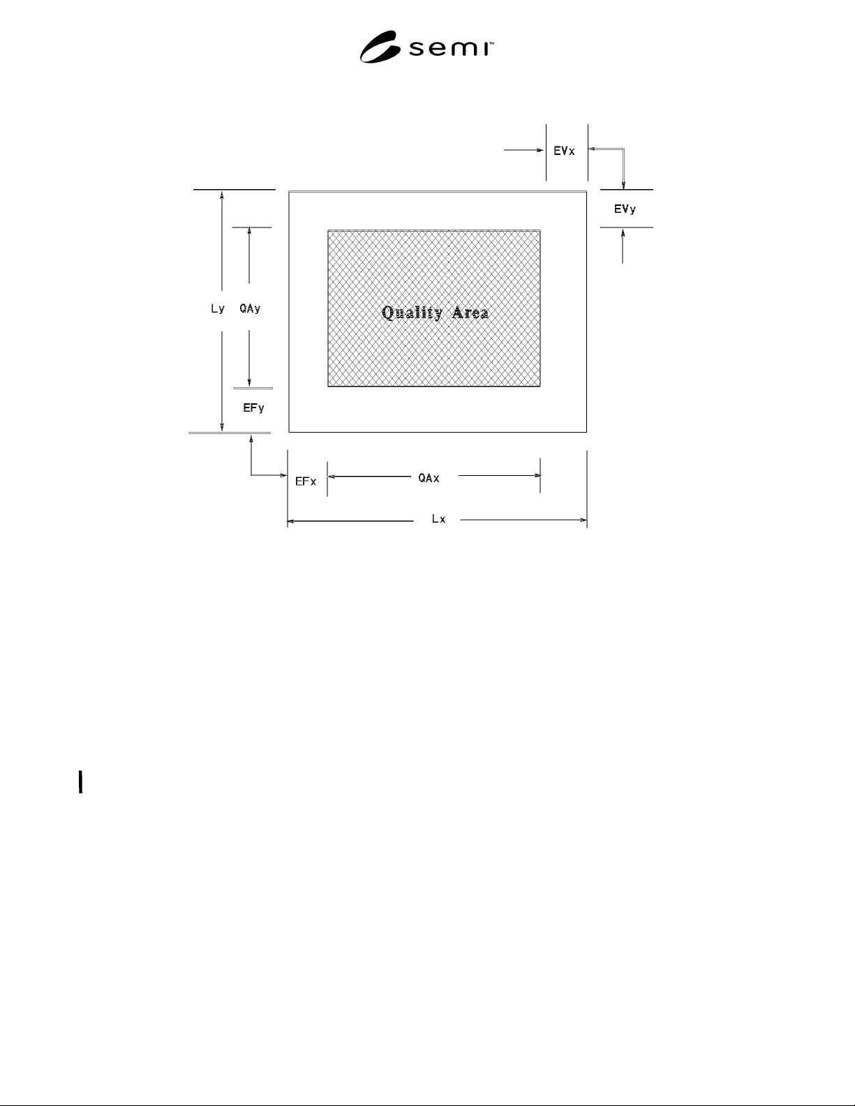
5.1 A substrate edge length is defined in two
dimensions, L
X
and L
Y
, with nominal and tolerance
values for each.
5.2 A quality area is defined by two dimensions, QA
X
and QA
Y
, with nominal and tolerance values for each.
5.3 A fixed edge exclusion area is defined for the
substrate edges to be placed against reference (also
called “banking”) pins.
5.4 Two variable edge exclusion areas result from
combining the above three dimension sets.
6 Procedure
6.1 Locate the properties in Sections 6.2–6.4 relative to
the substrate origin, using the nominal values assigned
by the substrate specification.
6.2 Let L
X
= the substrate edge length in the x-
direction, and
L
Y
= the substrate edge length in the y-direction. (See
Figure 1.)
6.3 Let EF
X
= the fixed edge exclusion area along the
substrate’s lower edge, and
EF
Y
= the fixed edge exclusion area along the
substrate’s left edge.
6.4 Let QA
X
= the quality area’s edge length in the x
direction, and
QA
Y
= the quality area’s edge length in the y direction.
6.5 Then EV
X
and EV
Y
, the variable edge exclusions,
are not specified. They result from the interaction of
substrate tolerance variations from nominal with the
fixed location origin.
SEMI D3-91 © SEMI 1991, 2003 2
L , L
QA , QA
EF , EF
EV , EV are not specified, but result from tolerance effects.
X
X
X
X
Y
Y
Y
Y
are specified, nominal dimensions
Figure 1
Substrate Area Relationships
NOTICE: SEMI makes no warranties or representations as to the suitability of the standards set forth herein for any
particular application. The determination of the suitability of the standard is solely the responsibility of the user.
Users are cautioned to refer to manufacturer’s instructions, product labels, product data sheets, and other relevant
literature respecting any materials mentioned herein. These standards are subject to change without notice.
The user’s attention is called to the possibility that compliance with this standard may require use of copyrighted
material or of an invention covered by patent rights. By publication of this standard, SEMI takes no position
respecting the validity of any patent rights or copyrights asserted in connection with any item mentioned in this
standard. Users of this standard are expressly advised that determination of any such patent rights or copyrights, and
the risk of infringement of such rights, are entirely their own responsibility.
Copyright by SEMI® (Semiconductor Equipment and Materials
International), 3081 Zanker Road, San Jose, CA 95134. Reproduction o
f
the contents in whole or in part is forbidden without express written
consent of SEMI.