semi合集-English.pdf - 第4478页
SEMI D17-0200 © SEMI 1998, 2000 13 Figure 7 Cassette Physical Alignm ent Interface – Type B Roller Shape
SEMI D17-0200 © SEMI 1998, 2000 12
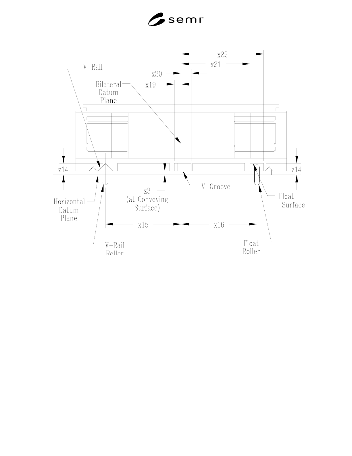
Figure 6
Cassette Physical Alignment Interface – Type B
Roller Position
SEMI D17-0200 © SEMI 1998, 200013
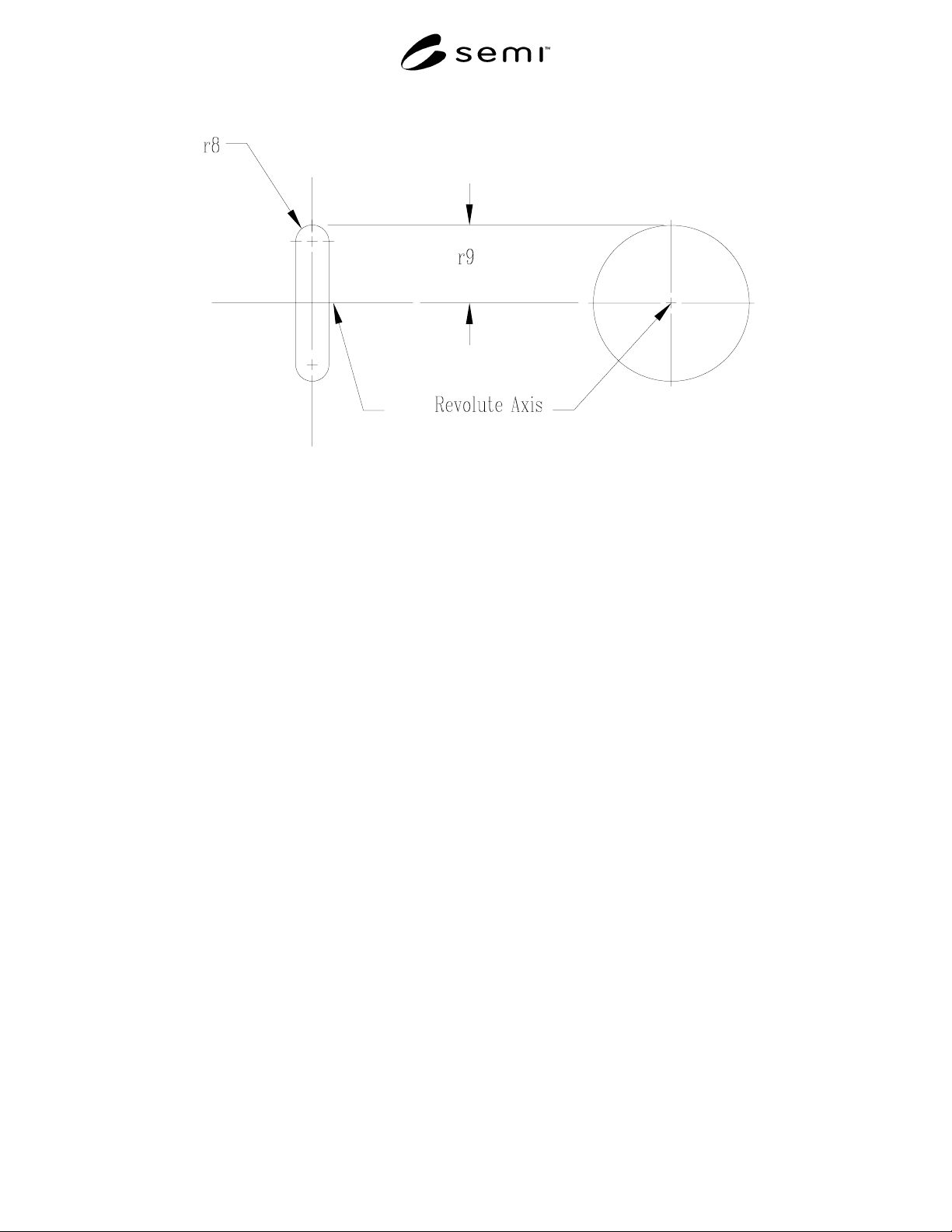
Figure 7
Cassette Physical Alignment Interface – Type B
Roller Shape
SEMI D17-0200 © SEMI 1998, 2000 14
APPENDIX 1
NOTE: The material in this appendix is an official part of SEMI D17 and was approved by full letter ballot procedures on
December 15, 1999 by the North American Regional Standards Committee. Determination of the suitability of the material
herein is solely the responsibility of the user.
A1-1 Application Notes
A1-1.1 The shape of the teeth holding the substrates is not specified in this standard. The tooth surface that touches
the substrate should have a large radius to minimize stress on the substrate and tooth.
A1-1.2 Extra clearance (larger than the pitch) has been added below the bottom substrate (for non-random
sequential access to the substrates with a faster or less precise robot). To increase the stability of Type A Cassettes,
the points on the cassette bottom that are the most distant from the lines connecting each pair of coupling pins
should be made as close as practical to the horizontal datum plane so that the cassette cannot tip very far off of the
kinematic coupling.
NOTICE: SEMI makes no warranties or representations as to the suitability of the standards set forth herein for
any particular application. The determination of the suitability of the standard is solely the responsibility of the user.
Users are cautioned to refer to manufacturer’s instructions, product labels, product data sheets, and other relevant
literature respecting any materials mentioned herein. These standards are subject to change without notice.
The user’s attention is called to the possibility that compliance with this standard may require use of copyrighted
material or of an invention covered by patent rights. By publication of this standard, SEMI takes no position
respecting the validity of any patent rights or copyrights asserted in connection with any item mentioned in this
standard. Users of this standard are expressly advised that determination of any such patent rights or copyrights, and
the risk of infringement of such rights, are entirely their own responsibility.
Copyright by SEMI® (Semiconductor Equipment and Materials
International), 3081 Zanker Road, San Jose, CA 95134. Reproduction o
f
the contents in whole or in part is forbidden without express written
consent of SEMI.