semi合集-English.pdf - 第4834页
SEMI M1-0305 © SEMI 1978, 2005 10 Table 1 Silicon Wafer Specification Fo rmat for Order Entry , Parts 1 and 2 Part 1 General Information ITEM INFORMATION Date: Customer Name Purchase Order Number Line Number Item Number …

SEMI M1-0305 © SEMI 1978, 2005 9
5.3.1 Lot acceptance procedures.
5.3.2 Certification (if required).
5.3.3 Packing and shipping container labeling requirements.
5.4 Finally, many other characteristics may be specified in purchase orders for silicon wafers.
5.4.1 These shall be selected from the other items listed in the Silicon Wafer Specification Format for Order Entry,
Parts 1 and 2 (see Table 1).
5.4.1.1 The parameter values provided in the requirements tables in §6 may be used to identify appropriate values in
the specification without selecting a value for each line. However, even if these requirements table values are used,
the desired test methodology must be selected in accordance with ¶5.2.
5.4.2 It is essential that all choices for the items selected to be specified be made in order not to have unspecified
parameters that would lead to surprises between supplier and customer. This is particularly important in the
specification of wafer site flatness, for which a variety of parameters must be selected as outlined in Appendix 1.
5.4.3 Of the various items listed, the following (listed in the order in which they appear in Table 1) are most often
selected, especially for wafers to be used for advanced integrated circuit manufacture:
nominal edge exclusion (to define the fixed quality area),
structural characteristics,
wafer ID marking,
total thickness variation (TTV or GBIR),
warp (and sometimes bow or sori),
site flatness (SFQR), and
localized light scatterers (LLS).
6 Requirements
6.1 General Characteristics
6.1.1 The crystal growth method shall be modified Czochralski (Cz), float zone (FZ), or magnetic Czochralski
(MCz) as specified on the purchase order. In some cases, the supplier is given the option of selecting Cz or MCz.
6.1.1.1 If the Cz or MCz method is used for crystal growth, it may be permissible to utilize refined (previously
melted) polysilicon in the growth charge; when this is the case, the appropriate box should be checked..
6.1.2 The crystal orientation shall be as specified on the purchase order. Usually either (100) or (111) is specified,
but (110) is sometimes specified for polished wafers to be used for making SOI wafers. Occasionally, another
orientation, such as (311) or (511), is specified.
6.1.3 The conductivity type shall be either n or p.
6.1.4 The dopant shall be specified to match the conductivity type. In general, boron (B) is used for p-type
material, while phosphorus (P) is most commonly used for n-type material. For some applications, antimony (Sb) or
arsenic (As) are used to obtain
n-type wafers. For high power applications, neutron transmutation doping is often
used to obtain high resistivity n-type wafers.
6.1.5 The nominal edge exclusion, EE, specifies the diameter of the fixed quality area (FQA), which is given by the
nominal diameter minus 2·EE (see Figure 1). This quantity provides a center-referenced property.
SEMI M1-0305 © SEMI 1978, 2005 10
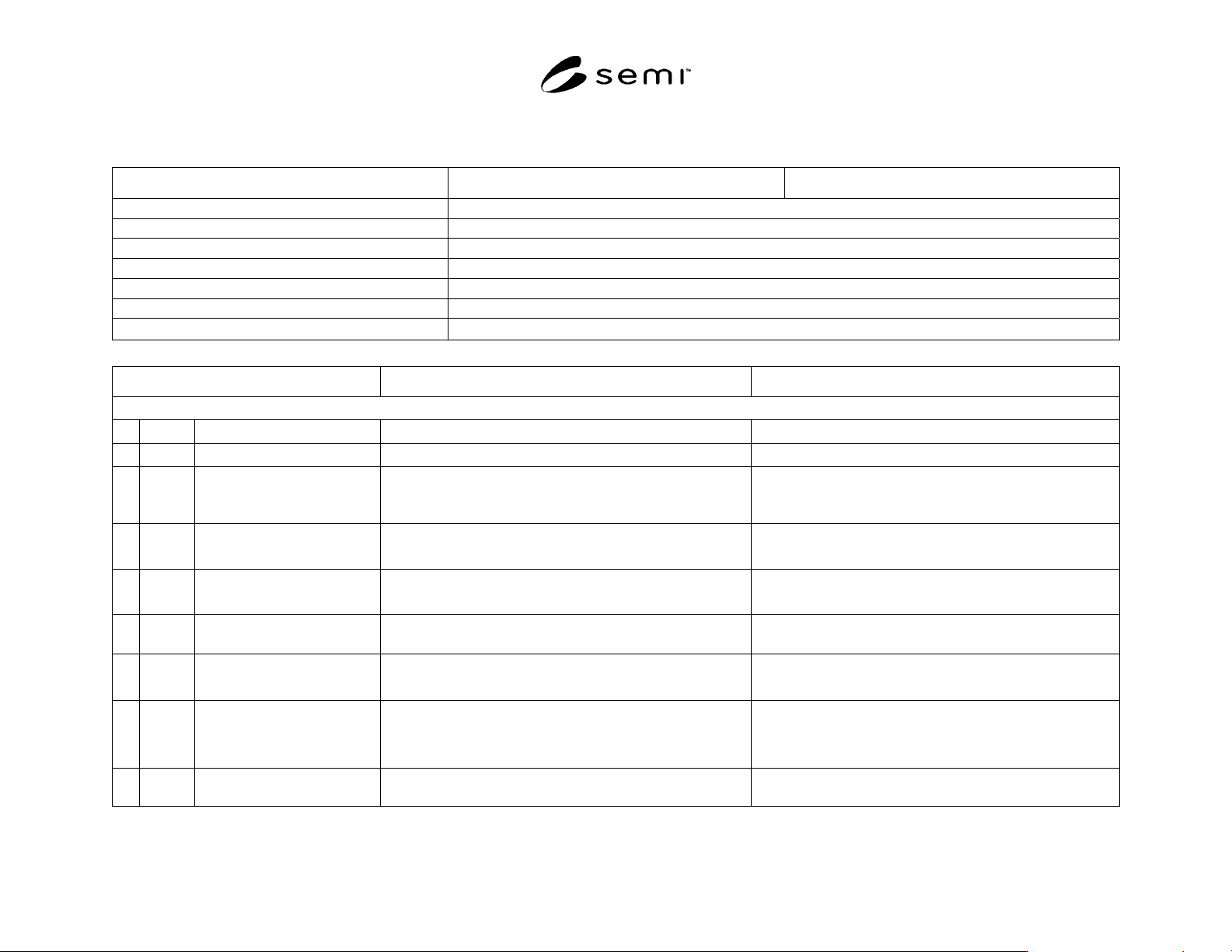
Table 1 Silicon Wafer Specification Format for Order Entry, Parts 1 and 2
Part 1 General Information
ITEM INFORMATION Date:
Customer Name
Purchase Order Number
Line Number
Item Number
General Specification Number
Revision Level
Part Number/Revision
Part 2 Polished Wafer or Substrate
ITEM SPECIFICATION MEASUREMENT METHOD
2-1. GENERAL CHARACTERISTICS (Note that indicates a required item for which a value or choice must be indicated in order to minimally specify a silicon wafer.)
2-1.1 Growth Method [ ]Cz; [ ]FZ; [ ]MCz; [ ]Supplier option of Cz or MCz
2-1.2 Use of Refined Polysilicon [ ]Permitted; [ ]Not permitted
2-1.3 Crystal Orientation [ ](100); [ ](111); [ ](110); [ ]Other: (specify) ( )
[ ]SEMI MF26 (X-Ray); [ ] SEMI MF26 (Optical);
[ ]JEITA EM-3501; [ ]DIN 50433/1; [ ]DIN 50433/2;
[ ]DIN 50433/3; [ ]Other: (specify)____________
2-1.4 Conductivity Type [ ]p; [ ]n
[ ]SEMI MF42; [ ]JIS H 0607; [ ]DIN 50432;
[ ]Other: (specify)______
2-1.5 Dopant
[ ]B; [ ]P; [ ]Sb; [ ]As; [ ]Neutron Transmutation Doped;
[ ]Other: (specify) ______
2-1.6
Nominal Edge Exclusion
#1
(See Figure 1)
[ ]2 mm; [ ]3 mm; [ ]5 mm; [ ]Other: (specify)_______mm
2-1.7 Co-dopant in Crystal
[ ]None; [ ]Nitrogen; [ ]Carbon; [ ]Nitrogen and Carbon;
[ ]Argon; [ ]Other: (specify)__________
2-1.8 Wafer Surface Orientation
(with respect to crystal
orientation, see item 2-1.3)
[ ]On-orientation: [ ]0.00 ± 1.00; [ ]0.00 _____
[ ]Off-orientation: [ ]0.6 0.4 [ ]2.50 ± 0.50;
[ ]4.00 ± 0.50; [ ]_____ _____
[ ]SEMI MF26 (X-Ray); [ ] SEMI MF26 (Optical);
[ ]JEITA EM-3501; [ ]DIN 50433/1; [ ]DIN 50433/2;
[ ]DIN 50433/3; [ ]Other: (specify)_____________
2-1.9 Orthogonal Misorientation
(See Figure 2)
[ ] 5 max; [ ]Other: [ ], max
SEMI M1-0305 © SEMI 1978, 2005 11
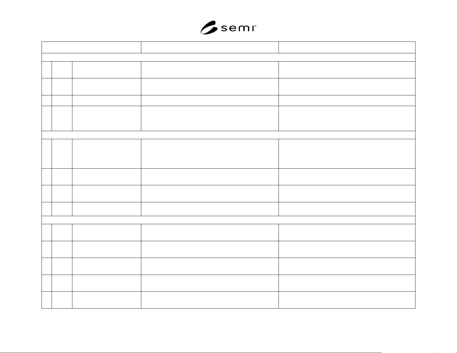
ITEM SPECIFICATION MEASUREMENT METHOD
2-2. ELECTRICAL CHARACTERISTICS (Note that indicates a required item for which a value or choice must be indicated in order to minimally specify a silicon wafer.)
2-2.1
Resistivity
Measured at
Nominal [ ] ± Tolerance [ ] ·cm
[ ]Center Point; [ ]Other: (specify)____________
[ ]SEMI MF84; [ ] SEMI MF673; [ ]DIN 50431
[ ]DIN50445; [ ]Other: (specify)____________
2-2.2
Radial Resistivity Variation
(RRG)
Not greater than [ ]%
SEMI MF81 Figure 1 [ ]A, [ ]B, [ ]C, [ ]D; [ ]DIN 50435;
[ ]Other: (specify) ______________
2-2.3 Resistivity Striations Not greater than [ ]% [ ]SEMI MF525; [ ]Other: (specify)__________
2-2.4 Minority Carrier Lifetime Greater than [ ] s
SEMI MF28 [ ]A, [ ]B; SEMI MF391 [ ]A, [ ]B;[ ]SEMI
MF1388; [ ]SEMI MF1535; [ ]JEITA EM-3502;
[ ]JIS H 0604; [ ]DIN 50440/1; [ ]Other: (specify)___________
2-3. CHEMICAL CHARACTERISTICS
2-3.1 Oxygen Concentration
(Values using the following
Calibration Factor, see
SEMI M44)
Nominal [ ] ± Tolerance [ ]; [ ]× 10
17
cm
3
; [ ]ppma
[ ]IOC-88; [ ] Old ASTM; [ ]New ASTM or Old DIN;
[ ] Original JEITA; [ ]Other: (specify)__________
IR (Interstitial): [ ] SEMI MF1188; [ ] SEMI MF1619;
[ ] JEIDA EM-3504; [ ] DIN 50438-1; [ ]Other:
(specify)_______
SIMS (Total): [ ] SEMI MF1366; [ ]GFA (Total)
2-3.2 Radial Oxygen Variation Not greater than [ ]% SEMI MF951 Plan [ ]A1; [ ]A2; [ ]A3; [ ]B; [ ]B1; [ ]C; [ ]D;
[ ]Other: (specify)______
2-3.3 Carbon Concentration
(Background, cf 2-1.7)
Not greater than [ ] [ ]ppma; [ ] × 10
16
cm
3
[ ] SEMI MF1391; JEITA EM-3503; [ ]DIN 50438/2;
[ ]Other: (specify)_______
2-3.4 Boron Concentration in
Heavily Doped n-type Silicon
Not greater than [ ] ppba
[ ]SEMI MF1528; [ ]Other: (specify)__________
2-4. STRUCTURAL CHARACTERISTICS
2-4.1 Dislocation Etch Pit Density [ ]Not greater than [ ]/cm
2
[ ]SEMI MF1809; [ ]JIS H 0609; [ ]DIN 50434;
[ ]DIN 50443/1; [ ]Other: (specify)_________
2-4.2 Slip [ ]None [ ]Other: (specify)________ [ ]SEMI MF1809; [ ]JIS H 0609; [ ]DIN 50434;
[ ]DIN 50443/1; [ ]Other: (specify)_________
2-4.3 Lineage [ ]None [ ]Other: (specify)________ [ ]SEMI MF1809; [ ]JIS H 0609; [ ]DIN 50434;
[ ]DIN 50443/1; [ ]Other: (specify)_________
2-4.4 Twin Boundary [ ]None [ ]Other: (specify)_______ [ ]SEMI MF1809; [ ]JIS H 0609; [ ]DIN 50434;
[ ]DIN 50443/1; [ ]Other: (specify)_________
2-4.5 Swirl [ ]Not greater than [ ]% of wafer area [ ]SEMI MF1809; [ ]JIS H 0609; [ ]DIN 50434;
[ ]DIN 50443/1; [ ]Other: (specify)_________