semi合集-English.pdf - 第4842页
SEMI M1-0305 © SEMI 1978, 2005 18 Fixed Qualit y Area EE = Nominal Edge Excl usion F Q A Boundary Nominal W afer Per iphery Primary Fl at Secondary Flat Fixed Qualit y Area EE = Nominal Edge Excl usion EE = Nominal Edge …
SEMI M1-0305 © SEMI 1978, 2005 17
ITEM SPECIFICATION MEASUREMENT METHOD
2-9.6 Stains [ ]None; [ ] Other: (specify)______________________ [ ]SEMI MF 523; [ ]JIS H 0614; [ ]Other: (specify)__________
2-9.7 Roughness [ ] ________ nm rms [ ] SEMI M40; [ ]Other: (specify)______________
2-9.8 Brightness (Gloss) [ ] ______________________ [ ]ASTM D 523; [ ]JIS Z 8741; [ ]Other: (specify)___________
2-9.9 Scratches – Macro [ ]None; [ ]Cum Length =[ ]mm [ ]SEMI MF 523; [ ]JIS H 0614; [ ]Other: (specify)__________
2-9.10 Scratches – Micro [ ]None; [ ]Cum Length =[ ]mm [ ]SEMI MF 523; [ ]JIS H 0614; [ ]Other: (specify)__________
2-9.11 Localized Light Scatterers
Size: [ ] m (LSE) Count: [ ] [ ] per wafer; [ ] per cm
2
Size: [ ] m (LSE) Count: [ ] [ ] per wafer; [ ] per cm
2
[ ]SEMI MF 523; [ ]JIS H 0614; [ ]SSIS
#4
;
[ ]Other: (specify)____
2-10. OTHER (as required)
#1
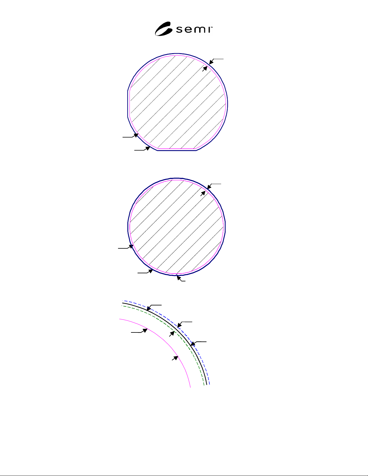
The nominal edge exclusion, EE, specifies the diameter of the FQA, which is given by the nominal diameter (see Item 2-6.1) minus 2EE (see Figure 1). This quantity provides a center referenced
property. Although use of edge referenced properties is discouraged, some equipments and procedures are based on edge referenced dimensions. When this occurs, the quality area is not fixed and
some part of the fixed quality area may fall outside the evaluated area, which is generally not a desirable situation.
#2
If specified as polished, this term is meant to imply a surface condition and not a particular processing technique. If desired, a quantitative measure of surface finish may optionally be indicated by
specifying the rms microroughness over a specified spatial frequency (or wavelength) range. Because a standardized test method has not yet been developed for this metric, both values and test
procedures, including sampling plan and detrending procedures, shall be agreed upon between supplier and customer.
#3
Flatness Acronyms are defined in the Flatness Decision Tree in Appendix 1.
#4
In today’s technology, it may be possible to inspect for some of these items using automated surface scanning inspection systems (SSIS). Such systems should be calibrated according to SEMI M53
using polystyrene latex spheres deposited in accordance with SEMI M58. Some indication of the defects separable by such instruments is provided in SEMI M35; however, a standard test procedure has
yet to be developed. Application of automated inspection with the use of an SSIS must be agreed upon between supplier and customer.
SEMI M1-0305 © SEMI 1978, 2005 18
Fixed Quality Area
EE = Nominal Edge Exclusion
F Q A Boundary
Nominal Wafer Periphery
Primary Flat
Secondary Flat
Fixed Quality Area
EE = Nominal Edge Exclusion
EE = Nominal Edge Exclusion
F Q A BoundaryF Q A Boundary
Nominal Wafer PeripheryNominal Wafer Periphery
Primary Flat
Secondary Flat
Notch
Nominal Wafer Periphery
F Q A Boundary
EE = Nominal Edge Exclusion
Fixed Quality Area
Notch
Notch
Nominal Wafer PeripheryNominal Wafer Periphery
F Q A BoundaryF Q A Boundary
EE = Nominal Edge ExclusionEE = Nominal Edge Exclusion
Fixed Quality AreaFixed Quality Area
EE = Nominal Edge Exclusion
A
ctual Wafer Periphery Limits
F Q A Boundary
Nominal Wafer Periphery
Fixed Quality Area
EE = Nominal Edge Exclusion
EE = Nominal Edge Exclusion
A
ctual Wafer Periphery Limits
A
ctual Wafer Periphery Limits
F Q A Boundary
F Q A Boundary
Nominal Wafer PeripheryNominal Wafer Periphery
Fixed Quality Area
c. Nominal and Actual Wafer Peripheries
b. Notched Wafer
a. Flatted Wafer
Figure 1
Fixed Quality Area
SEMI M1-0305 © SEMI 1978, 2005 19
6.1.5.1 This quantity is usually specified as 2 mm or 3 mm, but some advanced wafer processing technologies are
moving in the direction of 1 mm. However, it should be noted that not all processes and metrology can work as
close to the wafer edge as implied by the nominal edge exclusion.
6.1.5.2 In addition, it is sometimes necessary to specify additional exclusion zones, such as those for wafer
identification marks or wafer holding areas.
6.1.5.3 Although use of edge referenced properties is discouraged, some equipments and procedures are based on
edge referenced dimensions. When this occurs, the quality area is not fixed and some part of the fixed quality area
may fall outside the evaluated area, which is generally not a desirable situation.
6.1.6 A co-dopant may be required for polished wafers intended to be processed into annealed wafers. Some co-
dopants may also be used in connection with control of oxygen precipitation characteristics even when the wafer is
not annealed.
6.1.7 Wafer Surface Orientation — The wafer shall conform to the surface orientation as specified in the purchase
order.
6.1.7.1 For on-orientation wafers, the angular tolerance from the plane perpendicular to the growth axis shall be
specified.
6.1.7.2 For off-orientation wafers, both the misorientation angle from the growth axis and its angular tolerance shall
be specified.
6.1.7.2.1 A misorientation angle between 0.2 and 1.0 (0.6 0.4) from a (100) plane is frequently used for some
epitaxial substrates.
6.1.7.2.2 A misorientation angle of 2.50 or 4.00 0.5 from a (111) plane is often used for other epitaxial
substrates.
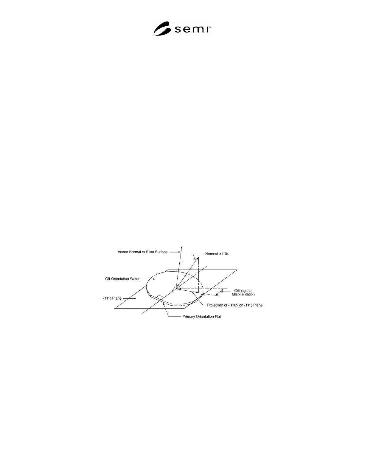
6.1.7.3 Orthogonal misorientation is the tilt angle of the normal to a (111) wafer surface toward nearest <110>
direction in a plane parallel with the primary flat as indicated in Figure 2.
NOTE: If the off-orientation angle is determined with the seed end up, the polished surface of the finished
wafer must be the surface toward the seed end, and vice versa. Polishing of the incorrect wafer surface
results in an incorrect wafer tilt, which can cause unwanted pattern shifts and distortions if the wafer is used
subsequently for epitaxial layer growth. Because the convention for determining the off-orientation angle is
not the same worldwide, it is essential to establish accurately the desired convention.
Figure 2
Orthogonal Misorientation of {111} Wafer
6.1.7.3.1 The contribution of 5 of orthogonal misorientation to the total off-orientation angle is less than 0.5.
6.1.7.4 For ion implant applications, the following tolerance issues should be considered:
6.1.7.4.1 For general use where channeling is to be avoided, the current wafer orientation specification of ±1.0
deviation from the [100] axis (perpendicular to the (100) plane of the wafer) is adequate. This specification is
suitable for minimum channeling applications, provided that the appropriate ion implant equipment angle settings
are employed.