semi合集-English.pdf - 第4980页
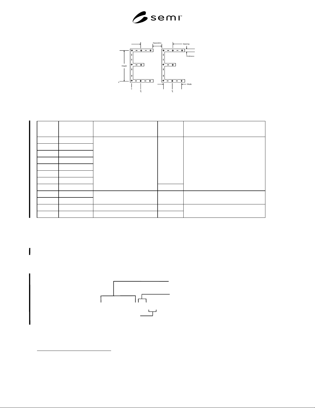
SEMI M12-1103 © SEMI 1988, 2003 2 Figure 1 Character Outline Table 2 Code Character Location CharacterStyle Parameter Code Definition 1 Alpha/Numeric 2 Alpha/Numeric 3 Alpha/Numeric 4 Alpha/Numeric 5 Alpha/Numeric 6 Alph…
SEMI M12-1103 © SEMI 1988, 2003 1
SEMI M12-1103
SPECIFICATION FOR SERIAL ALPHANUMERIC MARKING OF THE
FRONT SURFACE OF WAFERS
This specification was technically approved by the Global Traceability Committee and is the direct
responsibility of the North American Traceability Committee. Current edition approved by the North
American Regional Standards Committee on July 27, 2003. Initially available at www.semi.org October
2003; to be published November 2003. Originally published in 1988; previously published March 2003.
1 Purpose
1.1 This specification provides a serial alphanumeric
marking of silicon or other semiconductor wafers. The
wafer serial number links the properties of the wafer
stored in an appropriate database system to each
individual wafer for purposes of tracking and control
during wafer and device manufacture.
1.2 By defining the basic code used for the mark, this
specification ensures the consistency of wafer marking
performed by wafer manufacturers. Thus, it allows
simplification of the performance requirements of
automatic optical character reading (OCR) equipment,
provides for unassisted and immediate human
readability without wafer handling, and facilitates
resolution of wafer level process variations.
1.3 The marking code is intended to be valid for a
broad range of wafer products (i.e., epi, SOI, processed
polished wafers, etc.).
2 Scope
2.1 This specification defines the geometric and spatial
limits of the alphanumeric code, specifically for serial
identification of flatted and notched silicon wafers.
2.2 This specification does NOT address the marking
techniques that may be employed when complying with
this standard.
NOTICE: This standard does not purport to address
safety issues, if any, associated with its use. It is the
responsibility of the users of this standard to establish
appropriate safety and health practices and determine
the applicability of regulatory or other limitations prior
to use.
3 Referenced Standards
3.1 SEMI Standards
SEMI M13 — Specification for Alphanumeric Marking
of Silicon Wafers
NOTICE: Unless otherwise indicated, all documents
cited shall be the latest published versions.
4 Terminology
4.1 Definitions
4.1.1 adjacent character misalignment, R
adj
— the
vertical distance between the character baselines of two
adjacent characters on the same line.
4.1.2 character separation — the horizontal distance
between the adjacent boundaries of any two adjacent
characters.
4.1.3 character spacing — the horizontal distance
between the character centerlines of any two adjacent
characters.
4.1.4 character window — the rectangular window
within which all characters must be contained.
4.1.5 front surface of the wafer — the exposed surface
upon which active semiconductor devices have been or
will be fabricated.
4.1.6 line character misalignment, R
line
— the vertical
distance between the character baselines of the highest
and the lowest characters on the same line.
5 Shape and Size of Marking
5.1 Solid line or dot matrix method may be used to
write characters. The minimum matrix shall be 5 dots
horizontal and 9 dots vertical. More dots may be used,
up to and including a solid line. Higher density is
recommended to achieve improved read reliability (see
Related Information 1).
5.2 Character Dimensions and Spacing — (see Table 1
and Figure 1)
Table 1 Character Dimensions
Character mm
Height 1.624 ± 0.025
Width 0.812 ± 0.025
Thickness (See NOTE 1) 0.200 + 0.050/-0.150
Spacing 1.420 ± 0.025
NOTE 1: The thickness of the diagonal in the letter " N" is 0.138 ±
0.05 mm for single density dot matrix.
SEMI M12-1103 © SEMI 1988, 2003 2
Figure 1
Character Outline
Table 2 Code
Character
Location
CharacterStyle Parameter Code Definition
1 Alpha/Numeric
2 Alpha/Numeric
3 Alpha/Numeric
4 Alpha/Numeric
5 Alpha/Numeric
6 Alpha/Numeric
7 Alpha/Numeric
A through Z
and
0 through 9
8 Numeric Only
IDENTIFICATION NUMBER
0 through 9
Supplier-Assigned (see Note 1)
9 Alpha Only
10 Alpha Only
WAFER SUPPLIER
IDENTIFICATION
A through Z (see SEMI AUX001
1
and Note 1)
11 Alpha Only CHECK CHARACTER A
11
A through H
12 Numeric Only CHECK CHARACTER A
12
0 through 7
Error-Detecting Method (see Section 9)
NOTE 1: In the absence of information at any assigned location, a dash (–) must be used.
1 SEMI AUX001, List of Wafer Supplier Identification Codes, available from SEMI web site: www.semi.org.
6 Alphanumeric Code
6.1 The code consists of one line of 12 characters. The first eight characters are an identification number which is
unique to the wafer for a given vendor. These characters may be alphanumeric except character 8 which must be
numeric (see Table 2). Characters 9 and 10 comprise the supplier identification code (see SEMI AUX001
1
).
Characters 11 and 12 are check characters (see Section 9). These check characters are machine generated for code
acceptance and reading verification.
Identification Number
Wafer
Supplier
Identification
Code
Check Characters
12345678ABC1
Figure 2
Example of Code
6.2 In the absence of a character at any assigned location, a dash (–) must be used.
SEMI M12-1103 © SEMI 1988, 2003 3
6.3 An example of the code is given in Figure 2.
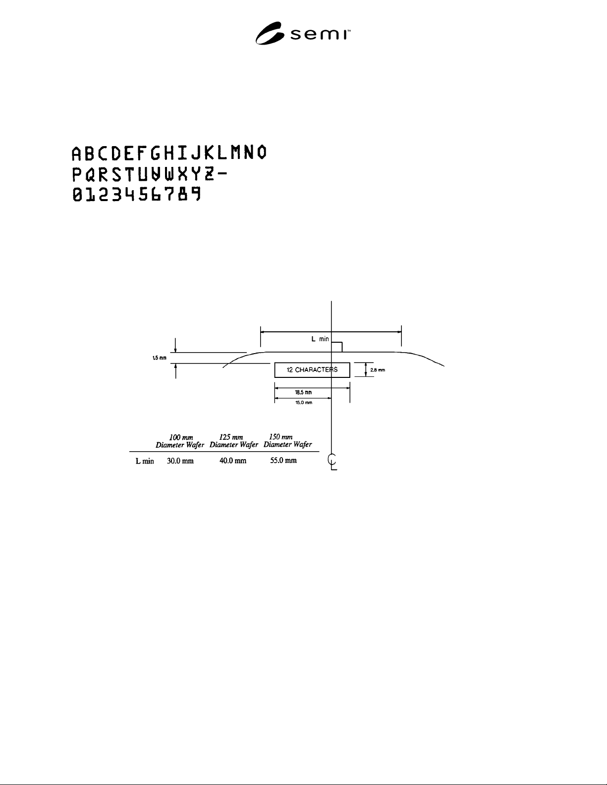
6.4 SEMI-OCR Standard Character Set — This character set contains capital letters from A to Z, numerals from 0
to 9, a dash, and a period (see Appendix 1). The period is NOT used in the code symbols defined in this
specification (see Tables 2 and 3), although it is required for use in the code symbols defined in SEMI M13.
Table 3 SEMI OCR Character Set Modified for Use in this Specification
7 Character Window
7.1 The character window must be located on the front surface of the wafers.
7.2 All characters must be contained within the character window dimensions specified in Figures 3 (for flatted
wafers) or Figure 4 (for notched wafers).
7.3 The top of the characters is toward the side of the character window nearest to the flat or notch.
Figure 3
Character Window Location for Flatted Wafers
NOTE: The vertical center line referenced in Figure 3 is the bisector of the primary fiducial (flat).