semi合集-English.pdf - 第5007页
SEMI M16-1103 © SEMI 1989, 2003 3 SEMI MF1389 — Test Methods for Photolumin escence Analysis of Single Crystal Silicon for III-V Impurities SEMI MF1391 — Test Method for Substitutio nal Carbon Content of Silicon by Infra…

SEMI M16-1103 © SEMI 1989, 2003 2
5 Ordering Information
5.1 Purchase orders for polysilicon furnished to this
specification shall include the following items:
5.1.1 Form (nugget, granular, or rod)
5.1.2 Shape and size distribution (nugget form only)
5.1.3 Purity
5.1.4 Surface texture (nugget form only)
5.1.5 Surface condition
5.1.6 Optionally, surface metal contamination
5.1.7 Appearance
5.1.8 Lot acceptance procedures (see Section 8 )
5.1.9 Certification (if required) (see Section 10 )
5.1.10 Packing and marking (see Section 11 )
6 Materials and Manufacture
6.1 The material shall consist of polysilicon with the
form specified in the purchase order or contract.
7 Physical Requirements
7.1 The material shall conform to the properties
specified in the purchase order or contract, as follows
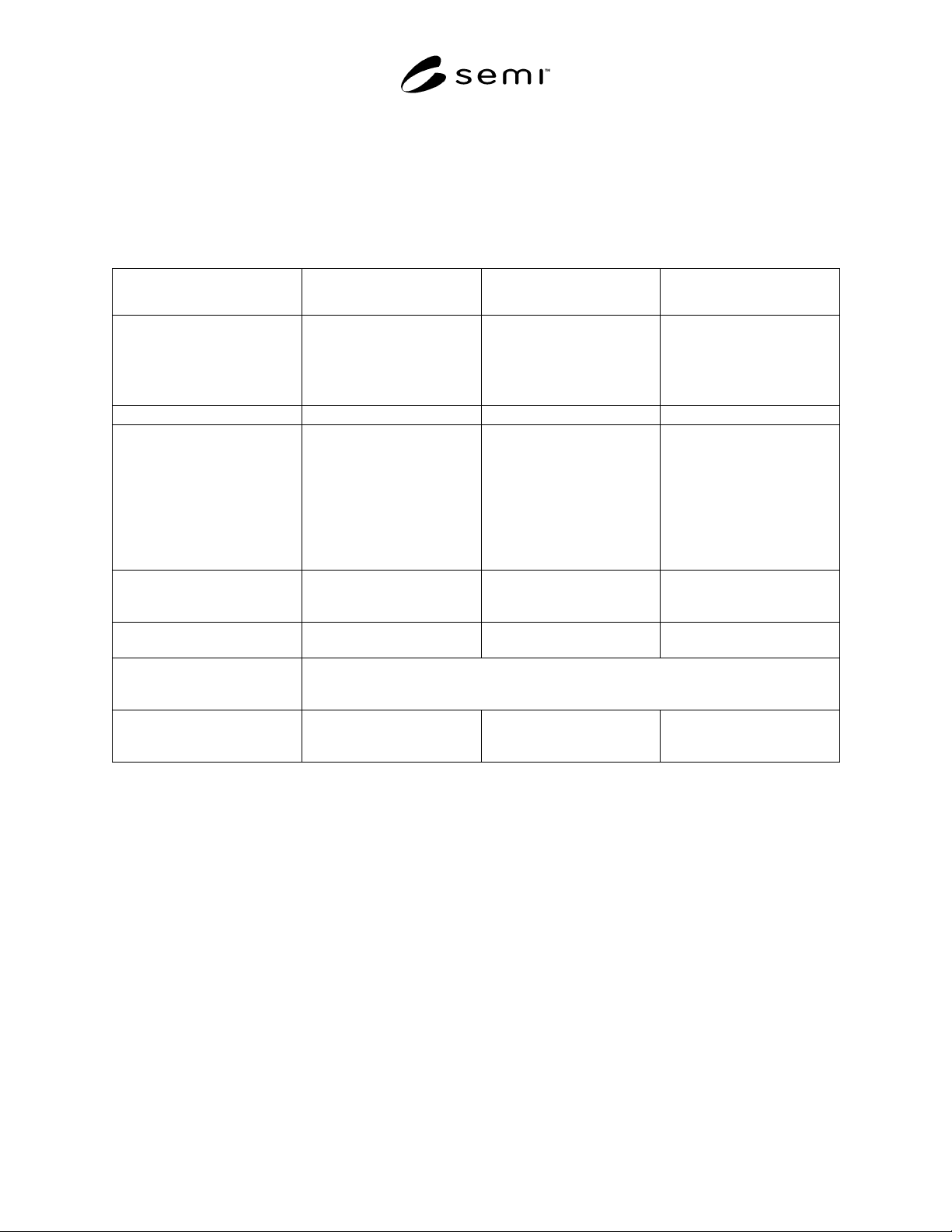
(see Table 1):
7.1.1 Shape and size distribution (nugget form only)
7.1.2 Purity
7.1.3 Surface texture (nugget form only)
7.1.4 Surface condition
7.1.5 Surface metal contamination, if specified
7.1.6 Appearance
8 Sampling
8.1 Unless otherwise specified, ASTM Practice E 122
shall be used. When so specified, appropriate sample
sizes shall be selected from each lot in accordance with
ANSI/ASQC Z1.4-1993. Inspection levels shall be
agreed upon between the supplier and the purchaser.
9 Test Methods
9.1 Shape and Size Distribution (Nugget Form Only)
— Determine by methods agreed upon by the purchaser
and the supplier.
9.2 Purity — For nugget and rod forms, determine in
accordance with SEMI MF1723. For granular form,
determine in accordance with SEMI MF1708.
9.3 Surface Texture (Nugget Form Only) — Determine
by a method agreed upon by the purchaser and the
supplier. Visual limit standards shall be used to
describe acceptable limits.
9.4 Surface Metal Contamination, if Specified —
Determine in accordance with SEMI MF1724.
9.5 Surface Condition — Identify as to whether or not
the surface has been etched.
9.6 Appearance — Inspect visually for stains, discolo-
ration, and visible contamination.
10 Certification
10.1 Upon request of the purchaser in the contract or
order, a manufacturer’s or supplier’s certification that
the material was manufactured and tested in accordance
with the specification shall be furnished at the time of
shipment (Certificate of Compliance). Upon request, a
report of the test results may also be required
(Certificate of Analysis).
10.2 In the interest of controlling inspection costs, the
supplier and the purchaser may agree that the material
shall be certified as “capable of meeting” certain
requirements. In this context, “capable of meeting”
shall signify that the supplier is not required to perform
the appropriate test in Section 9. However, if the
purchaser performs the test and the material fails to
meet the requirement, the material may be subject to
rejection.
11 Packing and Marking
11.1 Special packing requirements shall be subject to
agreement between the supplier and purchaser.
Otherwise all poly shall be handled, inspected, and
packed in bags and boxes in such a manner as to
minimize abrasion, chipping, and contamination, and in
accordance with the best industry practices to provide
ample protection against damage during shipment.
11.2 The poly supplied under the specification shall be
identified by appropriately labeling the outside of each
box and each bag therein. Identification shall include,
as a minimum, the weight and lot number of the
polysilicon. The lot number shall provide traceability
to information concerning the manufacturing history of
the particular poly in that lot. Such information shall be
kept on file at the manufacturer’s facility for at least
three years after that particular lot has been accepted by
the purchaser.
12 Related Documents
12.1 The following SEMI standards, cited in SEMI
MF1708 and MF1723 are required to perform the tests
described in those practices:
SEMI M16-1103 © SEMI 1989, 2003 3
SEMI MF1389 — Test Methods for Photoluminescence
Analysis of Single Crystal Silicon for III-V Impurities
SEMI MF1391 — Test Method for Substitutional
Carbon Content of Silicon by Infrared Absorption
SEMI MF1630 — Test Method for Low Temperature
FT-IR Analysis of Single Crystal Silicon for III-V
Impurities
SEMI MF1725 — Guide for Analysis of
Crystallographic Perfection of Silicon Ingots
Table 1 Requirements for Polysilicon
Property Nugget Form
(previously SEMI M16.1)
Granular Form Rod Form
Shape Irregular chunks, crushed from
polysilicon rods, with
maximum linear dimension of
150 mm.
As supplied;
Polysilicon granules are nearly
spherical in shape and range in
size from 200 to 2500 µm with
a mean size of about 900 µm.
Approximately cylindrical
polycrystalline rods, with
length equal to or greater than
the diameter of the rod.
Size Distribution As specified by customer. Not applicable. Not applicable.
Purity
Acceptor concentration, max in
parts per billion, atomic (ppba)
As specified by customer. As specified by customer. As specified by customer.
Donor concentration, max in
parts per billion, atomic (ppba)
As specified by customer. As specified by customer. As specified by customer.
Carbon concentration, max in
parts per million, atomic (ppma)
As specified by customer. As specified by customer. As specified by customer.
Evaluate in accordance with SEMI MF1723 SEMI MF1708 SEMI MF1723
Surface Texture Visual limit standards as
agreed upon between supplier
and purchaser.
Not applicable. Not applicable.
Surface Condition Identified as to whether or not
the nuggets have been etched.
As agreed upon between
supplier and purchaser.
Identified as to whether or not
the rods have been etched.
Surface Metal Contamination, if
specified
Sodium, Aluminum, Iron, Chromium, Copper, Nickel, Potassium, and Zinc, as specified, from
thin surface layer on the sample, determined in parts per billion by weight (ppbw) in
accordance with SEMI MF1724.
Appearance Clean with no stains,
discoloration, or visible
contamination.
As agreed upon between
supplier and purchaser.
Clean with no stains,
discoloration, or visible
contamination.
SEMI M16-1103 © SEMI 1989, 2003 4
RELATED INFORMATION 1
RELATIONSHIPS BETWEEN THE REQUIREMENTS OF SEMI M16 AND
THE REQUIREMENTS OF JEITA EM-3601
NOTICE: This related information is not an official part of SEMI M16. It was developed during the
revision of the document in May 2003. This related information was approved for publication by full letter
ballot on September 19, 2003.
R1-1 Introduction
R1-1.1 SEMI M16 and JEITA EM-3601 both provide
specification requirements for polycrystalline silicon
(poly) in nugget (chunk), granular, and rod forms.
R1-1.2 This related information section provides
comparisons between the two specifications with regard
both to the specification requirements and to the test
methods cited.
R1-2 Specification Requirements
R1-2.1 The philosophies of the two specifications are
quite different in that JEITA EM-3601 spells out
specific purity requirements, while SEMI M16 leaves
these to be “as specified by the customer.” The levels
specified in JEITA EM-3601 may serve as a starting
point for developing the necessary specifications.
R1-2.2 Purity Requirements
R1-2.2.1 JEITA EM-3601 lists the following bulk
purity requirements for the nugget and rod forms:
R1-2.2.1.1 Acceptor concentration, maximum:
• B 0.05 ppba
• Al 0.05 ppba
R1-2.2.1.2 Donor concentration, maximum:
• P 0.3 ppba
• As 0.05 ppba
R1-2.2.1.3 Carbon concentration, maximum:
• C 0.3 ppma
R1-2.2.2 JEITA EM-3601 lists the following bulk
purity requirements for the granular form:
• Total acceptors (B+ Al) 0.1 ppba, maximum
• Total donors (P+ As) 0.4 ppba, maximum
• Carbon 0.3 ppma, maximum
R1-2.2.3 JEITA EM-3601 lists the following surface
metal contamination requirements for the nugget and
granular forms (maximum surface metal contamination
levels are not listed for the rod form):
• Fe, Cr, Ni, and Na 3.0 ppbw, maximum
• Zn 1.0 ppbw, maximum
NOTE 2: These surface metal concentrations correspond to
1.5 ppba for Fe, Cr, and Ni; 3.8 ppma for Na; and 0.5 ppba for
Zn.
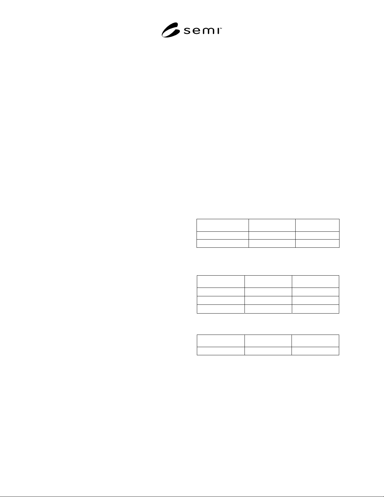
R1-2.3 Size Distribution — See Tables R1-1 through
R1-3.
Table R1-1 Size Requirements for Nugget Form
Poly
JEITA EM-3601 SEMI M16
Maximum Dimension 120 mm 150 mm
Minimum Dimension 10 mm not specified
Table R1-2 Size Requirements for Granular Form
Poly
JEITA EM-3601 SEMI M16
Maximum Size
3,500 µm 2,500 µm
Minimum Size
150 µm 200 µm
Mean Size not specified
~ 900 µm
Table R1-3 Size Requirements for Rod Form Poly
JEITA EM-3601 SEMI M16
Minimum Length not specified rod diameter
R1-3 Test Method Requirements
R1-3.1 Sample Preparation
R1-3.1.1 JEITA EM-3601 contains instructions for
preparing samples for photoluminescence, infrared
absorption, and atomic absorption spectroscopy
measurements. It cites the 1996 edition of JIS H 0615
for the preparation of samples from nugget and rod
forms for photoluminescence measurements.