semi合集-English.pdf - 第5064页
SEMI M21-0304 © SEMI 1992, 2004 9 RELATED INFORMATION 2 EXTENSIONS TO OTHER ELEMEN T ADDRESSING CONVENTIONS NOTICE: This related i nformation is not an official part of SEMI M21. It was de veloped during the original dev…
SEMI M21-0304 © SEMI 1992, 2004 8
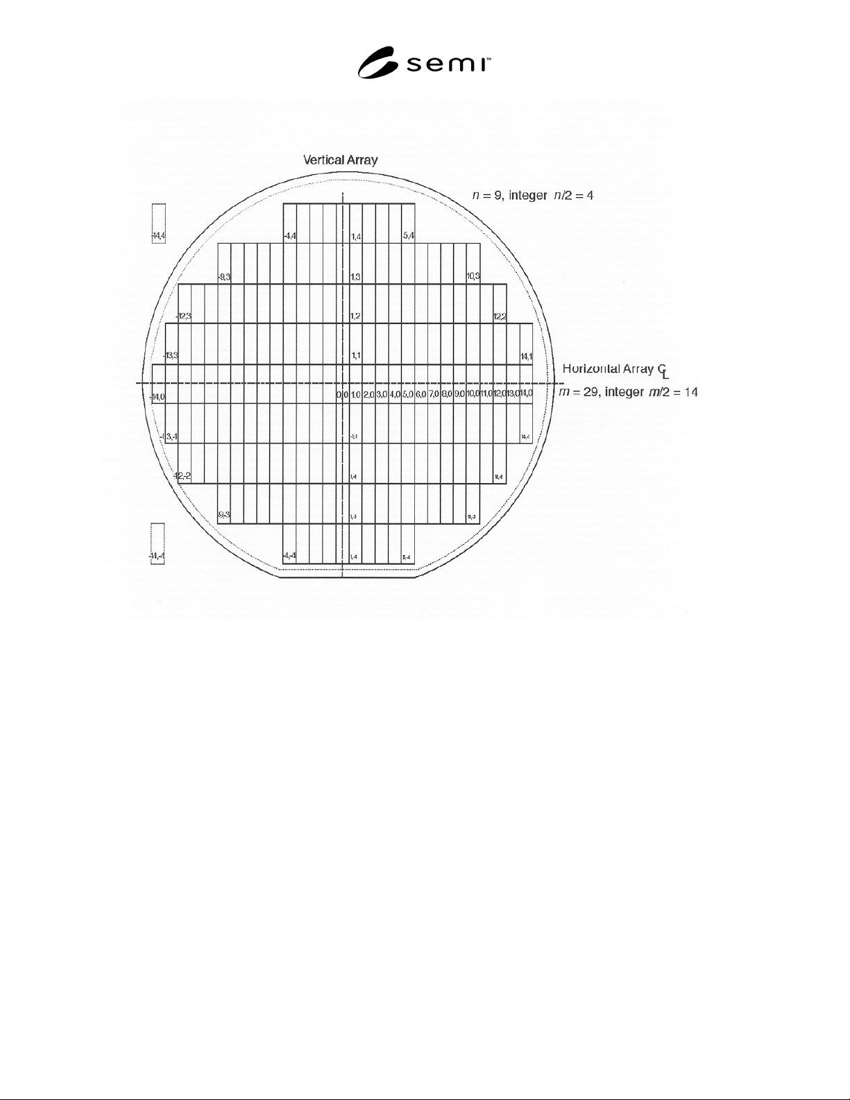
Figure R1-2
Truncated Array on the Wafer
SEMI M21-0304 © SEMI 1992, 2004 9
RELATED INFORMATION 2
EXTENSIONS TO OTHER ELEMENT ADDRESSING CONVENTIONS
NOTICE: This related information is not an official part of SEMI M21. It was developed during the
original development of the document. This related information was approved for publication by full
letter ballot on October 16, 2003.
R2-1 Element addressing conventions other than that
covered by this guide are also widely used in
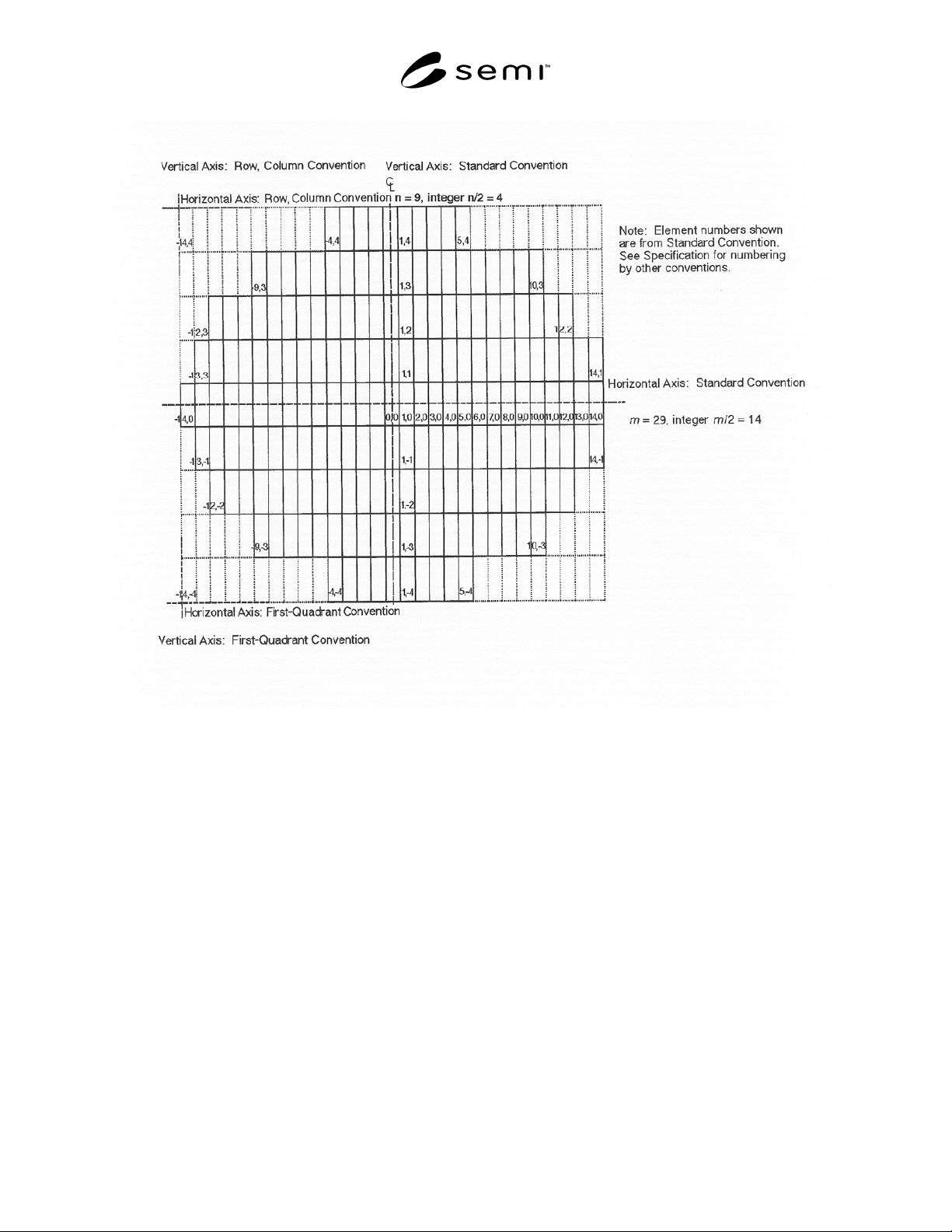
engineering. Two of these are illustrated in Figure R2-1
with the use of the same truncated array discussed in
Related Information 1.
R2-2 First-Quadrant Convention
R2-2.1 Addresses in this convention start at the lower
left corner of the array and increase to the right and
upward in the same way as in the convention covered
by this guide. The lower left corner of the array is
defined by the intersection of the bottom boundary of
the lowest row and the left boundary of the leftmost
column. In the case of tiling, the boundaries are those of
the lowest elements and the leftmost elements in the
array. The lower left corner may fall outside the useful
portion of the array. The lower left element of the array
is the element immediately to the right and above the
lower left corner of the array.
R2-2.2 The First-Quadrant Convention uses a column,
row address but does not have a zero row or a zero
column.
R2-2.3 The addresses of the corners of an array with m
columns and n rows in the First-Quadrant Convention
are as follows:
• lower left (Starting Element): (1,1)
• lower right: (m,1)
• upper left: (1,n)
• upper right: (m,n)
R2-2.4 The general formulas for obtaining the
addresses of any element (i
f
,j
f
) in the First-Quadrant
Convention from the addresses (i,j) in the convention
covered by this guide are as follows:
i
f
= i + integer(m/2) + 1
j
f
= j + integer(n/2) + 1
R2-2.5 These equations also apply to arrays with
column or row tiling if n
′
= n or m
′
= m, respectively. If
this condition is not met, the displacement of the row or
column which defines the array centerline with respect
to the boundary of the array must be known to
transform the addresses.
R2-3 Row, Column (Matrix) Convention
R2-3.1 Addresses in this convention start at the upper
left corner of the array and increase to the right and
downward. The upper left corner of the array is defined
by the intersection of the top boundary of the highest
row and the left boundary of the leftmost column. In the
case of tiling, the boundaries are those of the highest
elements and the leftmost elements in the array. The
upper left corner may fall outside the useful portion of
the array. The upper left element of the array is the
element immediately to the right and below the upper
left corner of the array.
R2-3.2 The Row, Column (Matrix) Convention uses a
row, column address and, like the First-Quadrant
Convention, does not have a zero row or a zero column.
R2-3.3 The addresses of the corners of an array with m
columns and n rows in the Row, Column (Matrix)
Convention are as follows:
• upper left (Starting Element): (1,1)
• upper right: (1,m)
• lower left: (n,1)
• lower right: (n,m)
R2-3.4 The general formulas for obtaining the
addresses of any element (i
m
,j
m
) in the Row, Column
(Matrix) Convention from the addresses (i,j) in the
convention covered by this guide are as follows:
i
m
=intege
r
n / 2
(
)
+
1
+
j
j
m
=integer m / 2
(
)
+
1
+
i
R2-3.5 These equations also apply to arrays with
column or row tiling if n
′
= n or m
′
= m, respectively. If
this condition is not met, the displacement of the row or
column which defines the array centerline with respect
to the boundary of the array must be known to
transform the addresses.
SEMI M21-0304 © SEMI 1992, 2004 10
Figure R2-1
Comparison of Array Addressing Conventions
NOTICE: SEMI makes no warranties or representations as to the suitability of the standards set forth herein for any
particular application. The determination of the suitability of the standard is solely the responsibility of the user.
Users are cautioned to refer to manufacturer’s instructions, product labels, product data sheets, and other relevant
literature respecting any materials mentioned herein. These standards are subject to change without notice.
The user’s attention is called to the possibility that compliance with this standard may require use of copyrighted
material or of an invention covered by patent rights. By publication of this standard, SEMI takes no position
respecting the validity of any patent rights or copyrights asserted in connection with any item mentioned in this
standard. Users of this standard are expressly advised that determination of any such patent rights or copyrights, and
the risk of infringement of such rights, are entirely their own responsibility.
Copyright by SEMI® (Semiconductor Equipment and Materials
International), 3081 Zanker Road, San Jose, CA 95134. Reproduction o
f
the contents in whole or in part is forbidden without express written
consent of SEMI.