semi合集-English.pdf - 第5075页
SEMI M23-0703 © SEMI 1993, 2003 4 9.10 Resistivity of Semi-insulating Wafers — Determined by ASTM Test Method F76 or SEMI M3 9 or DIN 50448. 9.11 Conductivity or Resistivity of Doped Wafers — Determined b y ASTM Test Met…

SEMI M23-0703 © SEMI 1993, 2003 3
describe the shape of groove that can be etched
perpendicular to the primary flat. The following are the
options of wafer surface orientation:
A. (100) ± 0.5° as shown in Figures 1 and 2
B. (100) off 2° toward any of the nearest (110) planes.
Examples
shown in Figures 3 and 4.
Direction of off-orientation can be designated by α
angle. (See Figure 5)
Figure 5 illustrates orthogonal misorientation.
5.1.5 Lot acceptance procedures (see Section 8),
5.1.6 Certification (see Section 11),
5.1.7 Packing and Marking (see Section 12).
5.2 Optional Criteria — The following items may be
specified optionally in addition to those listed above:
5.2.1 Crystal growth method,
5.2.2 Etch Pit Density (EPD) of Crystal,
5.2.3 Crystal Growth Perfection,
5.2.4 Impurity Type,
5.2.5 Surface Condition of Wafer,
5.2.6 Edge Profile (see Figures 6 and 7),
5.2.7 Mobility,
5.2.8 Resistivity, and
5.2.9 Carrier Concentration.
6 Materials and Manufacture
6.1 The material shall consist of wafers from ingots
grown to the material defined in the purchase order or
contract.
7 Physical and Electrical Requirements
7.1 The material shall conform to the crystallographic
orientation details as specified in the applicable
polished indium phosphide wafer standard.
7.2 The material shall conform to the details specified
in the purchase order or contract as follows:
7.2.1 Conduction Type,
7.2.2 Dopant,
7.2.3 Carrier Concentration,
7.2.4 Resistivity,
7.2.5 Etch Pit Density,
7.2.6 Mobility,
7.2.7 Surface Characteristics, and
7.2.8 Growth Methods.
8 Sampling
8.1 Unless otherwise specified, ASTM Practice E122
shall be used. When so specified, appropriate sample
sizes shall be selected from each lot in accordance with
ANSI/ASQC Z1.4-1993. Each quality characteristic
shall be assigned an acceptable quality level (AQL) or
lot total percent defective (LTPD) value in accordance
with ANSI/ASQC Z1.4-1993 definitions for critical,
major, and minor classifications. If desired and so
specified in the contract or order, each of these
classifications may alternatively be assigned cumulative
AQL or LTPD values. Inspection levels shall be agreed
upon between the supplier and the purchaser.
9 Test Methods
4
9.1 Diameter — Determined by ASTM Test Method
F613.
9.2 Thickness, Center Point — Determined by ASTM
Test Method F533.
9.3 Flat Length — Determined by ASTM Test Method
F671.
9.4 Flat Orientation
5
— Determined by etching
method identified in the appropriate InP wafer standard.
9.5 Total Thickness Variation — Determined by
ASTM Test Method F533 or F657.
9.6 Surface Orientation — Determined by ASTM Test
Method F26.
9.7 Orthogonal Misorientation — Determined by a
method agreed upon between the supplier and
purchaser.
9.8 Surface Defects and Contamination — Determined
by ASTM Test Methods F154, F523 or a method
agreed upon between the supplier and purchaser.
9.9 Mobility — Determined by ASTM Test Methods
F76 or SEMI M39.
4 InP wafers are extremely fragile. While the mechanical
dimensions of a wafer can be measured by use of tools such as a
micrometer calipers and other conventional techniques, the wafer
may be damaged physically in ways that are not immediately evident.
Special care must, therefore, be used in the selection and execution of
measurement methods.
5 Relating to the etchant used for identifying V-groove and/or
dovetail direction, see reference: “HBr-K2 Cr2O7 – H2O etching
system for indium phosphide” J.L. Weyher, et al. Materials Science
and Engineering B28 (1994) 488-492.

SEMI M23-0703 © SEMI 1993, 2003 4
9.10 Resistivity of Semi-insulating Wafers —
Determined by ASTM Test Method F76 or SEMI M39
or DIN 50448.
9.11 Conductivity or Resistivity of Doped Wafers —
Determined by ASTM Test Method F76 or F84 or
F673.
9.12 Carrier concentration — Determined by ASTM
Test Method F76 or F1392 or F1393 or Electrochemical
CV
6
.
9.13 Conductivity Type — Determined by ASTM Test
Method F42 or F76.
9.14 Crystal Perfection — Determined by a method
agreed upon between the supplier and purchaser.
9.15 Edge Contouring — Determined by ASTM Test
Method F928.
9.16 Bow — Determined by ASTM Test Method F534
or a method agreed upon between the supplier and
purchaser.
9.17 Etch Pit Density (EPD) — Determined by DIN
Standard Test Method 50454-2
10 Standard Defect Limits
10.1 Limits are determined by an agreement between
supplier and purchaser.
11 Certification
11.1 A manufacturer' s or supplier' s certification that
the material was manufactured and tested in accordance
with this specification, together with a report of the test
results. A certification shall be furnished at the time of
shipment, upon the request of the purchaser in the
contract or order.
6 NOTE: Electrochemical CV test method has not been completed
but is in the process of being developed by the industry.
12 Packing and Marking
12.1 Special packing and marking requirements shall
be subject to agreement between the supplier and the
purchaser. Otherwise, all wafers shall be handled,
inspected, and packed with the best industry practices
to provide ample protection against damage during
shipment.
12.2 The wafers supplied under these specifications
shall be identified by appropriately labeling the outside
of each box or other container and each subdivision that
the wafers will be stored prior to further processing.
Identification shall include lot number and wafer
number. Per the agreement between the supplier and
purchaser, the following must be accessible from the lot
and wafer numbers: nominal diameter, conductive
dopant, orientation, resistivity, and EPD. Such
information shall be retained on file at the
manufacturer' s facility for at least one month or as
negotiated between vendor and user after that particular
lot has been accepted by the purchaser.
13 Related Documents
“HBr-K
2
Cr
2
O
7
– H
2
O etching system for indium phos-
phide” J.L. Weyher, et al. Materials Science and
Engineering B28 (1994) 488-492.
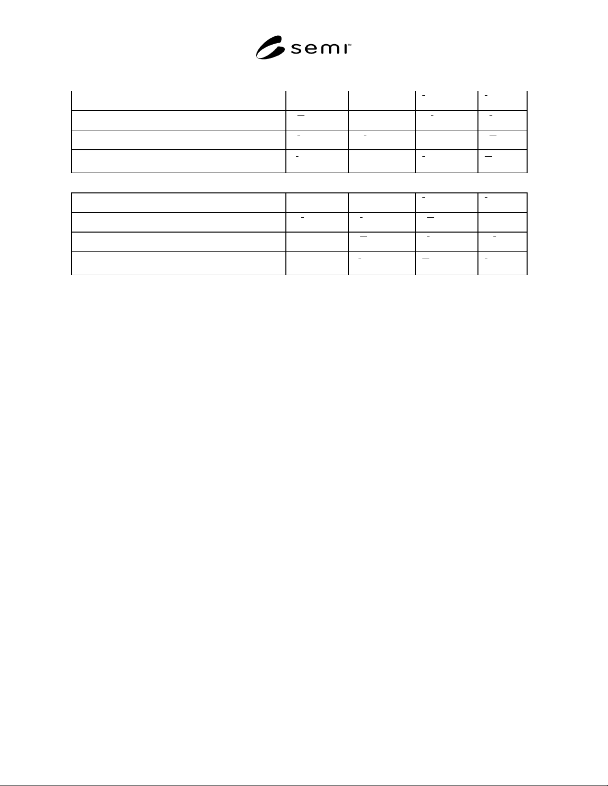
SEMI M23-0703 © SEMI 1993, 2003 5
Table 1 Equivalent Orientations — Dove-Tail Option
Surface orientation:
(100) (100)
)001( )001(
Primary flat location:
)110(
(011)
)101( )110(
Secondary flat location:
)110( )101(
(011)
)110(
For Surface orientation B, the off-orientation tilt direction
is toward: (See NOTE 1)
)011(
(110)
)101( )011(
Table 2 Equivalent Orientation — V-Groove Option
Surface orientation:
(100) (100)
)001( )001(
Primary flat location:
)101( )110( )110(
(011)
Secondary flat location:
(011)
)110( )110( )101(
For Surface orientation B, the off-orientation tilt direction
is toward:
(110)
)011( )011( )101(
The Symmetry of InP crystal structure allows other Miller indices to be used for identifying surface and flat orientations. This table lists various
possibilities that meet requirements for the above specific option.
NOTE 1: For Dove-Tail Option, any of the 110 tilt directions are considered equivalent.