semi合集-English.pdf - 第5097页
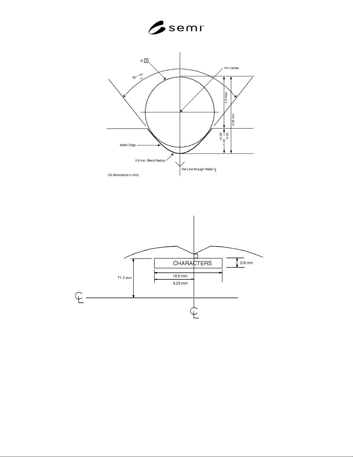
SEMI M23.6-0703 © SEMI 2003 6 Figure 5 Notch Dimensions Figure 6 Character Window L ocation NOTICE: SEMI makes no warran ties or representations as to the suitability of the standards set forth herein for any particular …
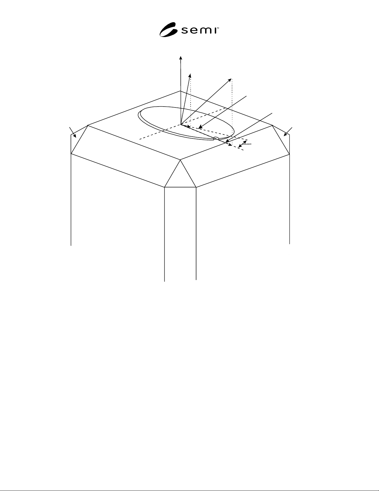
SEMI M23.6-0703 © SEMI 2003 5
(111) In
Vector Normal
to Wafer Surface
(100)
Orthogonal
Misorientation
Vector Normal
to (100) Plane
_
(101)
_
(001)
_
(011)
(010)
_
_
(111)
In
(110)
Vector Normal
to (110) Plane
Projection of Wafer Surface
Normal on (100) Plane
Projection of [110] on (100) Plane
_
(111)
P
Figure 4
Notched InP Wafer Illustrating Surface Orientation B, with Tilt and Orthogonal Misorientation
SEMI M23.6-0703 © SEMI 2003 6
Figure 5
Notch Dimensions
Figure 6
Character Window Location
NOTICE: SEMI makes no warranties or representations as to the suitability of the standards set forth herein for
any particular application. The determination of the suitability of the standard is solely the responsibility of the user.
Users are cautioned to refer to manufacturer’s instructions, product labels, product data sheets, and other relevant
literature respecting any materials mentioned herein. These standards are subject to change without notice.
The user’s attention is called to the possibility that compliance with this standard may require use of copyrighted
material or of an invention covered by patent rights. By publication of this standard, SEMI takes no position
respecting the validity of any patent rights or copyrights asserted in connection with any item mentioned in this
standard. Users of this standard are expressly advised that determination of any such patent rights or copyrights, and
the risk of infringement of such rights, are entirely their own responsibility.
Copyright by SEMI® (Semiconductor Equipment and Materials
International), 3081 Zanker Road, San Jose, CA 95134. Reproduction o
f
the contents in whole or in part is forbidden without express written
consent of SEMI.

SEMI M24-1103 © SEMI 1994, 2003 1
SEMI M24-1103
SPECIFICATION FOR POLISHED MONOCRYSTALLINE SILICON
PREMIUM WAFERS
This specification was technically approved by the Global Silicon Wafer Committee and is the direct
responsibility of the Japanese Silicon Wafer Committee. Current edition approved by the Japanese Regional
Standards Committee on August 8, 2003. Initially available at www.semi.org October 2003; published
November 2003. Originally published in 1994; previously published November 2001.
1 Purpose
1.1 This document specifies requirements for virgin
silicon premium wafers with nominal diameter from
150 mm to 300 mm used for particle counting, metal
contamination monitoring, and measuring pattern
resolution in the photolithography process in
semiconductor manufacturing. The premium wafer has
tighter specification values in some specific items for
the specific usage, and looser or equal specification
values in other items than a prime wafer has.
2 Scope
2.1 This specification classifies premium wafers
according to surface condition and dimensional
tolerances. Premium wafer classifications are
summarized in Table 1.
2.2 Specification values are determined by the use for
which the wafers are intended.
2.3 This specification provides premium wafers that
can be used to test and evaluate leading edge device
process.
2.4 For referee purposes, SI (System International)
units shall be used.
NOTICE: This standard does not purport to address
safety issues, if any, associated with its use. It is the
responsibility of the users of this standard to establish
appropriate safety and health practices and determine
the applicability of regulatory or other limitations prior
to use.
3 Referenced Standards
3.1 SEMI Standards
SEMI M1 — Specifications for Polished Mono-
crystalline Silicon Wafers
SEMI M18 — Format for Silicon Wafer Specification
Form for Order Entry
SEMI M20 — Specification for Establishing a Wafer
Coordinate System
SEMI M25 — Specification for Silicon Wafers for
Calibration of Light Point Defect Wafer Inspection
Systems with Respect to the Diameter of Polystyrene
Latex Spheres
3.2 ANSI Standard
1
ANSI/ASQC Z1.4 — Sampling Procedures and Tables
for Inspection by Attributes
3.3 ASTM Standards
2
D 523 — Standard Test Method for Specular Gloss
E 122 — Standard Practice for Choice of Sample Size
to Estimate the Average Quality of a Lot or Process
F 26 — Standard Test Methods for Determining the
Orientation of a Semiconductive Single Crystal
F 42 — Standard Test Methods for Conductivity Type
of Extrinsic Semiconducting Materials
F 84 — Standard Test Method for Measuring
Resistivity of Silicon Wafers with an In-Line Four-
Probe Array
F 154 — Standard Practices and Nomenclature for
Identification of Structures and Contaminants Seen on
Specular Silicon Surfaces
F 391 — Standard Test Methods for Minority-Carrier
Diffusion Length in Extrinsic Semiconductors by
Measurement of Steady-State Surface Photovoltage
F 523 — Standard Practice for Unaided Visual
Inspection of Polished Silicon Wafer Surface
F 533 — Standard Test Method for Thickness and
Thickness of Variation of Silicon Wafers
F 534 — Standard Test Method for Bow of Silicon
Wafers
F 613 — Standard Test Method for Measuring
Diameter of Semiconductor Wafers
1 American National Standards Institute, Headquarters: 1819 L
Street, NW, Washington, DC 20036, USA. Telephone: 202.293.8020;
Fax: 202.293.9287, New York Office: 11 West 42nd Street, New
York, NY 10036, USA. Telephone: 212.642.4900; Fax:
212.398.0023, Website: www.ansi.org
2 American Society for Testing and Materials, 100 Barr Harbor
Drive, West Conshohocken, Pennsylvania 19428-2959, USA.
Telephone: 610.832.9585, Fax: 610.832.9555, Website:
www.astm.org