semi合集-English.pdf - 第5161页
SEMI M31-0705 © SEMI 1998, 2005 21 APPENDIX 1 APPLICATION NOTES NOTICE: This appe ndix is an official par t of SEMI M31 and was a pproved by full lett er ballot procedures on July 15, 1999. A1-1 Although FOSB parameters …
SEMI M31-0705 © SEMI 1998, 2005 20
z
61
15
z
60
= 8 ± 0.5
y
64 = 42.1 ± 0.5
z
62
18
y
62
28
y
65
104
facial
datum plane
horizontal datum plane
of load port
y
63 = 37.3 ± 0.5
= 30
± 0.5°
z
63 = 7.5
± 0.5
r 61
16 (above
z
60)
r 60 = 16 ± 0.5 (below
z
60)
front side of the box
where wafers are accessed
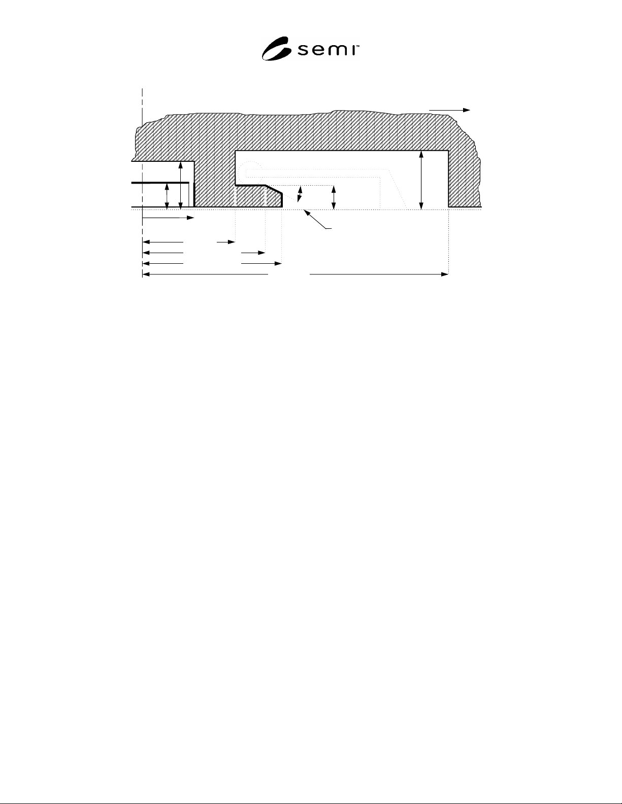
Figure 14
Side View of Retaining Features on Bottom of FOSB
6 Related Documents
6.1 SEMI Standards
SEMI E22.1 — Cluster Tool Module Interface 300 mm: Transport Module End Effector Exclusion Volume
Standard
SEMI E63 — Mechanical Specification for 300 mm Box Opener/Loader to Tool Standard (BOLTS-M) Interface
SEMI M28 — Specification for Developmental 300 mm Diameter Polished Single Crystal Silicon Wafers
NOTICE: Unless otherwise indicated, all documents cited shall be the latest published versions.

SEMI M31-0705 © SEMI 1998, 2005 21
APPENDIX 1
APPLICATION NOTES
NOTICE: This appendix is an official part of SEMI M31 and was approved by full letter ballot procedures on
July 15, 1999.
A1-1 Although FOSB parameters supporting effective reuse and cleaning (washing/drying) are not defined in this
document, it is essential that these capabilities be considered for a successful overall shipping box design.
A1-2 It is important to note that shipping boxes containing wafers are typically bagged for shipment to the IC
manufacturer. It is therefore important to design the outer surfaces of the shipping box to be compatible with this
common practice.
A1-3 Information about Automated-shippable Door
A1-3.1 When Automated-shippable door is used, the following contents should be understood for wafer quality.
A1-3.2 Rear of Door (y51): Increasing the value of y51, might have impact to the capability for absorbing drop
shock and wafer rotation during transportation, especially for x-direction since decreasing the area of holding wafer
by front wafer retainer.
A1-4 Items which need to be considered for automated-shippable door closing and opening process:
A1-4.1 When close or open the automated-shippable door by SEMI E62 compliant load port, not only SEMI E62
defined f30 and f34, but also consideration of other factors which may not be defined by SEMI E62, such as speed,
acceleration and deceleration of door closing and opening, are needed.
A1-4.2 Excessive f34 may cause deformation of the box, as well as breakage of wafers which are contained in the
box. Door may be closed with lesser f34 by deploying designs which utilize door and box related forces, such as
latch key torque.
A1-4.3 It needs to be considered that door may rebound at door opening process.
A1-4.4 Retaining features force (f61): It is noted that strong clamping force may produce plastic deformation.
NOTICE: SEMI makes no warranties or representations as to the suitability of the standards set forth herein for any
particular application. The determination of the suitability of the standard is solely the responsibility of the user.
Users are cautioned to refer to manufacturer's instructions, product labels, product data sheets, and other relevant
literature respecting any materials mentioned herein. These standards are subject to change without notice.
The user's attention is called to the possibility that compliance with this standard may require use of copyrighted
material or of an invention covered by patent rights. By publication of this standard, SEMI takes no position
respecting the validity of any patent rights or copyrights asserted in connection with any item mentioned in this
standard. Users of this standard are expressly advised that determination of any such patent rights or copyrights, and
the risk of infringement of such rights, are entirely their own responsibility.
Copyright by SEMI® (Semiconductor Equipment and Materials
International), 3081 Zanker Road, San Jose, CA 95134. Reproduction of
the contents in whole or in part is forbidden without express written
consent of SEMI.

SEMI M32-0998 © SEMI 1998, 2004 1
SEMI M32-0998 (Reapproved 0704)
GUIDE TO STATISTICAL SPECIFICATIONS
This guide was technically reapproved by the Global Silicon Wafer Committee and is the direct responsibility
of the North American Silicon Wafer Committee. Current edition reapproved by the North American
Regional Standards Committee on March 14, 2004. Initially available at www.semi.org May 2004; to be
published July 2004. Originally published September 1998.
1 Purpose
1.1 Specifications are based on requirements
negotiated between trading partners. This document
describes an explicit specification form that defines the
risk level as a part of parametric specifications. This
approach uses process capability information to focus
quality improvement efforts, reduce sampling, and
maintain low risks. It is based on the fundamental belief
that specifications should facilitate the movement
toward processed-in quality instead of inspected-in
quality.
1.2 It is important for users and suppliers to
acknowledge and mutually agree on quality levels so
the methods employed will satisfy their expectations.
Statistical specifications provide a convenient way to
do this.
1.3 Statistical specifications are designed to facilitate
the movement toward processed-in quality. They are
most appropriate for processes that have been
statistically characterized. This means the shape of the
statistical distribution that created the product is known,
or can be approximated to the satisfaction of the user
and the supplier. It also implies that the statistical
control of the process and the measurement systems are
defined to the level that is necessary to meet the current
needs.
2 Scope
2.1 This guide may be used when changing or adding
specifications to SEMI M18.
2.2 Statistical specifications apply to all processes that
have been statistically characterized. Solutions are
given for two product distribution shapes (normal &
lognormal), and the advantages of these solutions are
explained. Appendix 3 shows the statistically
characterized shape for many common silicon wafer
processes.
2.3 This guide applies to processes related to the
production and use of silicon wafers. It may also be
applied to the production and use of other materials.
2.4 This approach implies that the quality level shipped
is the same as the quality level produced.
2.5 This methodology can be an effective tool for
driving quality improvement.
2.6 This procedure can be coupled with other
techniques for centering the mean and reducing the
variation within the process distribution as deemed
necessary by the user and supplier.
2.7 Appendix 4 further explains the rationale for this
approach.
NOTICE: This standard does not purport to address
safety issues, if any, associated with its use. It is the
responsibility of the users of this standard to establish
appropriate safety and health practices and determine
the applicability of regulatory or other limitations prior
to use.
3 Limitations
3.1 Outlier effects are beyond the scope of this
document.
4 Referenced Standard
4.1 SEMI Standard
SEMI M18 — Format for Silicon Wafer Specification
Form for Order Entry
NOTICE: Unless otherwise indicated, all documents
cited shall be the latest published versions.
5 Terminology
5.1 Abbreviations and Acronyms
5.1.1 Cpk — process capability index
5.1.2 ppm — parts per million
5.2 Definitions
5.2.1 capability based sampling — any method that
uses the process capability as a factor in determining
the required sampling.
5.2.2 ECPK — process capability index on a non-
normal process which is corrected for non-normality.
5.2.3 error — the difference between the quality level
committed to a user and the level that could be
received.
5.2.4 process capability index (Cpk) — the smaller of
(upper spec limit - mean) ÷ 3 sigma, or (mean - lower
spec limit) ÷ 3 sigma.